
Method for growing GaN-based LED (Light Emitting Diode) on patterned substrate

A technology of LED epitaxial wafers and graphic substrates, which is applied in crystal growth, single crystal growth, single crystal growth, etc., can solve the problems of poor antistatic ability and large leakage current of epitaxial wafers, so as to improve the light extraction effect and prolong the service life , The effect of reducing the leakage current

Inactive Publication Date: 2014-09-10
XIANGNENG HUALEI OPTOELECTRONICS
View PDF3 Cites 0 Cited by
  • Summary
  • Abstract
  • Description
  • Claims
  • Application Information

AI Technical Summary

Problems solved by technology

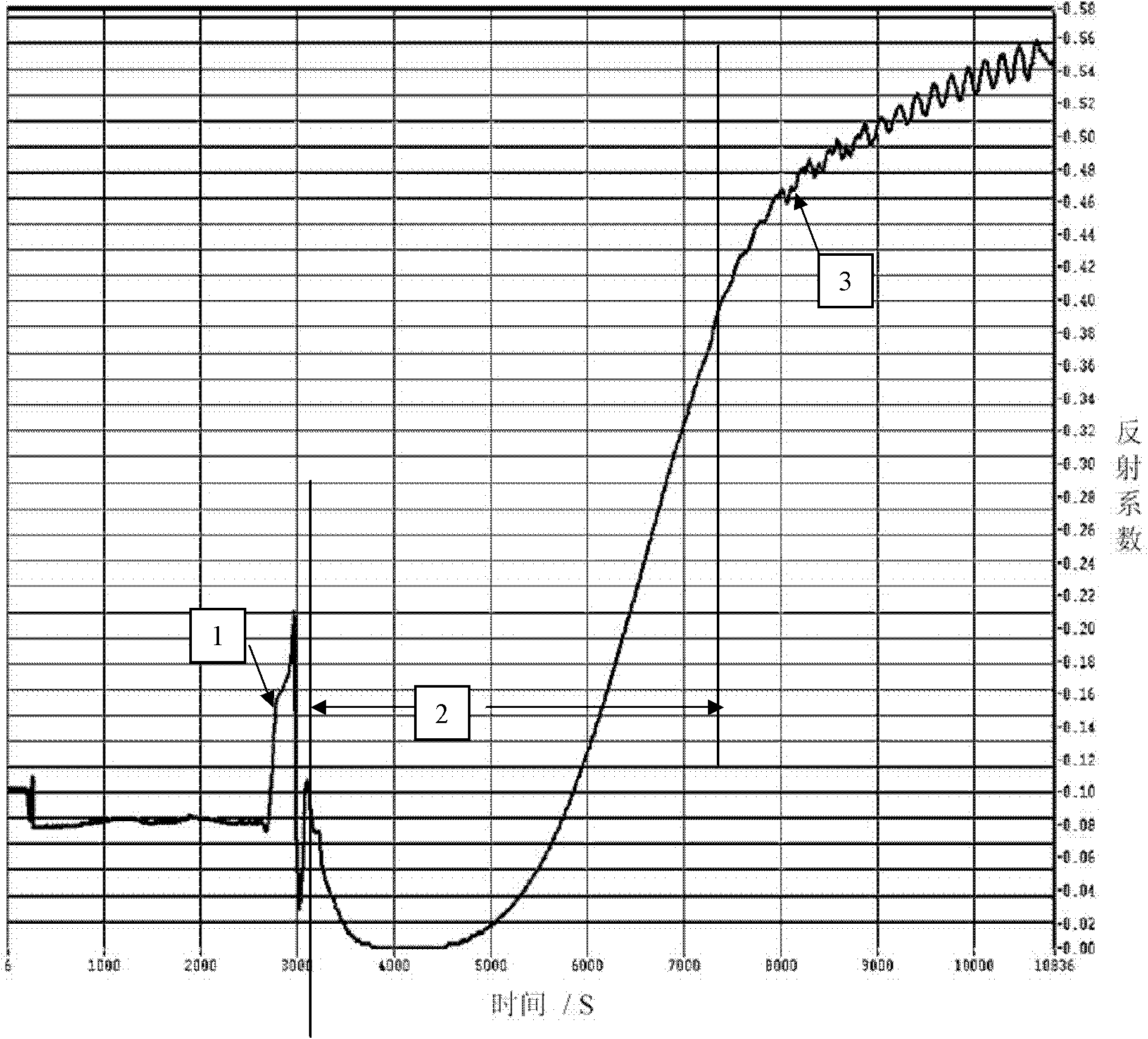
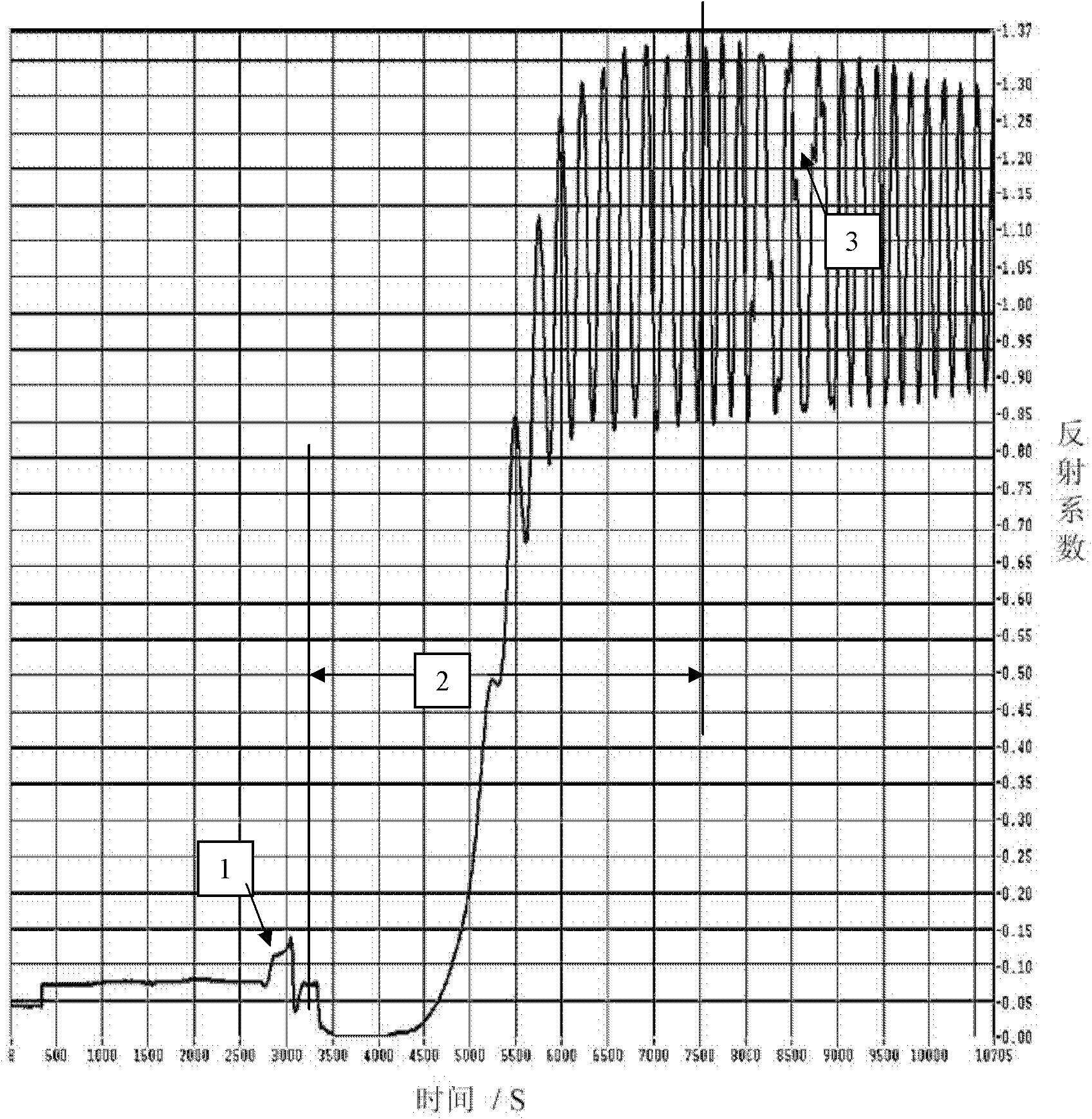
[0016] The invention provides a method for growing GaN-based LED epitaxial wafers on a graphic substrate to solve the problems of poor antistatic ability and large leakage current of existing epitaxial wafers

Method used


Image

  • Method for growing GaN-based LED (Light Emitting Diode) on patterned substrate
  • Method for growing GaN-based LED (Light Emitting Diode) on patterned substrate
  • Method for growing GaN-based LED (Light Emitting Diode) on patterned substrate

Examples


Embodiment 1

[0059] 1. Add O to the reaction chamber 2 , its content is 10ppm, where O 2 Added to the reaction chamber in a mixed form with nitrogen, and O in the mixed gas 2 The content is 25%;

[0060] 2. High temperature treatment: In the MOCVD reaction chamber, high-purity H 2 , reduce the pressure of the reaction chamber to 150 mbar, heat the patterned substrate to 1100 ° C, and treat at high temperature for 15 minutes;

[0061] 3. Nitriding treatment: cool down to 700°C, and pass NH into the reaction chamber 3 The flow rate is 10 standard liters / minute, and the time is 100 seconds, and the pattern substrate is nitrided;

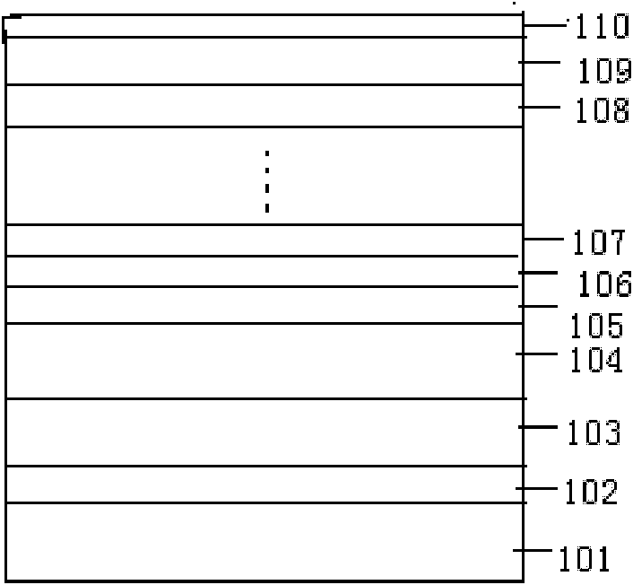
[0062] 4. Growth nucleation layer (such as figure 1 middle layer 102): reduce the temperature to 500°C in H 2 Under the atmosphere, a low-temperature buffer layer GaN with a thickness of 30 nanometers (such as figure 1 Middle 102nd Floor), NH 3 The flow rate is 10 standard liters / minute, and the flow rate of TMGa is 3×10 -4 mol / min, H 2 The flow rate is 80...

Embodiment 2

[0072] 1. Add O to the reaction chamber 2 and Cl 2 , its content is 5000ppm, where O 2 and Cl 2 Added to the reaction chamber in a mixed form with nitrogen, and O in the mixed gas 2 and Cl 2 The content is 40%;

[0073] 2. High temperature treatment: In the MOCVD reaction chamber, high-purity H 2 , reduce the pressure of the reaction chamber to 150 mbar, heat the patterned substrate to 1100 ° C, and treat at high temperature for 15 minutes;

[0074] 3. Nitriding treatment: cool down to 700°C, and pass NH into the reaction chamber 3 The flow rate is 10 standard liters / minute, and the time is 100 seconds, and the pattern substrate is nitrided;

[0075] 4. Growth nucleation layer (such as figure 1 middle layer 102): reduce the temperature to 500°C in H 2 Under the atmosphere, a low-temperature buffer layer GaN with a thickness of 30 nanometers (such as figure 1 Middle 102nd Floor), NH 3 The flow rate is 10 standard liters / minute, and the flow rate of TMGa is 3×10 -4 m...

Embodiment 3

[0078] 1. Add CO into the reaction chamber, the content of which is 10000ppm, wherein CO and nitrogen are added into the reaction chamber in a mixed form, and the content of CO in the mixed gas is 50%;

[0079] 2. High temperature treatment: In the MOCVD reaction chamber, high-purity H 2 , reduce the pressure of the reaction chamber to 150 mbar, heat the patterned substrate to 1100 ° C, and treat at high temperature for 15 minutes;

[0080] 3. Nitriding treatment: cool down to 700°C, and pass NH into the reaction chamber 3 The flow rate is 10 standard liters / minute, and the time is 100 seconds, and the pattern substrate is nitrided;

[0081] 4. Growth nucleation layer (such as figure 1 middle layer 102): reduce the temperature to 500°C in H 2 Under the atmosphere, a low-temperature buffer layer GaN with a thickness of 30 nanometers (such as figure 1 Middle 102nd Floor), NH 3 The flow rate is 10 standard liters / minute, and the flow rate of TMGa is 3×10 -4 mol / min, H 2 Th...


PUM

PropertyMeasurementUnit
thicknessaaaaaaaaaa
thicknessaaaaaaaaaa

Abstract

The invention provides a method for growing a GaN-based LED (Light Emitting Diode) on a patterned substrate. The method comprises the steps of high-temperature treatment, nitrogen treatment and nucleating layer forming by growing. Oxidizing gases are introduced into a reaction chamber before the step of high-temperature treatment, in the steps of high-temperature treatment and the nitrogen treatment or the nucleating layer forming by growing, wherein the oxidizing gases are one or more of CO, Cl2, O2, N2O and HCl. According to the method, the quality of an integral crystal lattice of an epitaxial wafer is improved; the brightness and the antistatic effect of the epitaxial wafer are improved; the leakage current is reduced; and the service life of the LED is prolonged.

Description

technical field [0001] The invention relates to the display field, in particular to a method for growing GaN-based LED epitaxial wafers on a pattern substrate. Background technique [0002] GaN-based high-brightness light-emitting diodes (LEDs) are ubiquitous in life and can be seen everywhere. Their applications include traffic lights, mobile phone backlights, outdoor full-color displays, urban landscape lighting, automotive interior and exterior lights, tunnel lights, etc. . With the continuous improvement of the brightness of GaN-based LEDs, LEDs have changed from traditional small to now achievable power-based household lighting. As a high-efficiency, environmentally friendly, green new solid-state lighting source, LED has the advantages of low voltage, low power consumption, small size, light weight, long life, and high reliability, and is being rapidly and widely used. [0003] At present, the epitaxial growth of GaN-based semiconductor materials is the most importan...

Claims


Application Information

Patent Timeline
Patent Type & Authority Patents(China)
IPC IPC(8): C30B29/38C30B25/02H01L33/00
Inventor 陈康梁智勇苗振林
Owner XIANGNENG HUALEI OPTOELECTRONICS
Learn More