
LED chip packaging structure, its manufacturing method, and display device

Active Publication Date: 2015-03-24
BOE TECH GRP CO LTD +1
View PDF3 Cites 0 Cited by
  • Summary
  • Abstract
  • Description
  • Claims
  • Application Information

AI Technical Summary

Benefits of technology

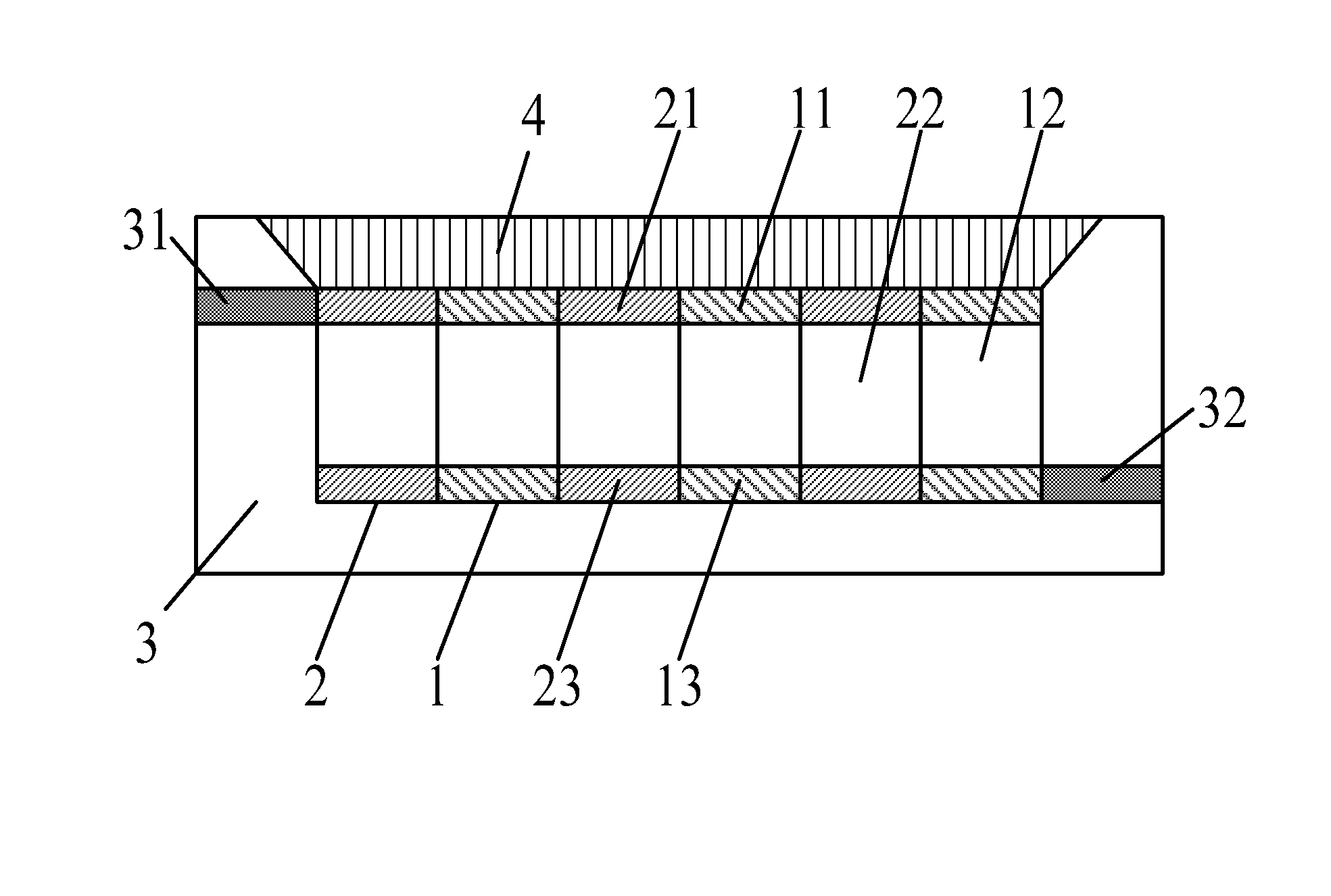
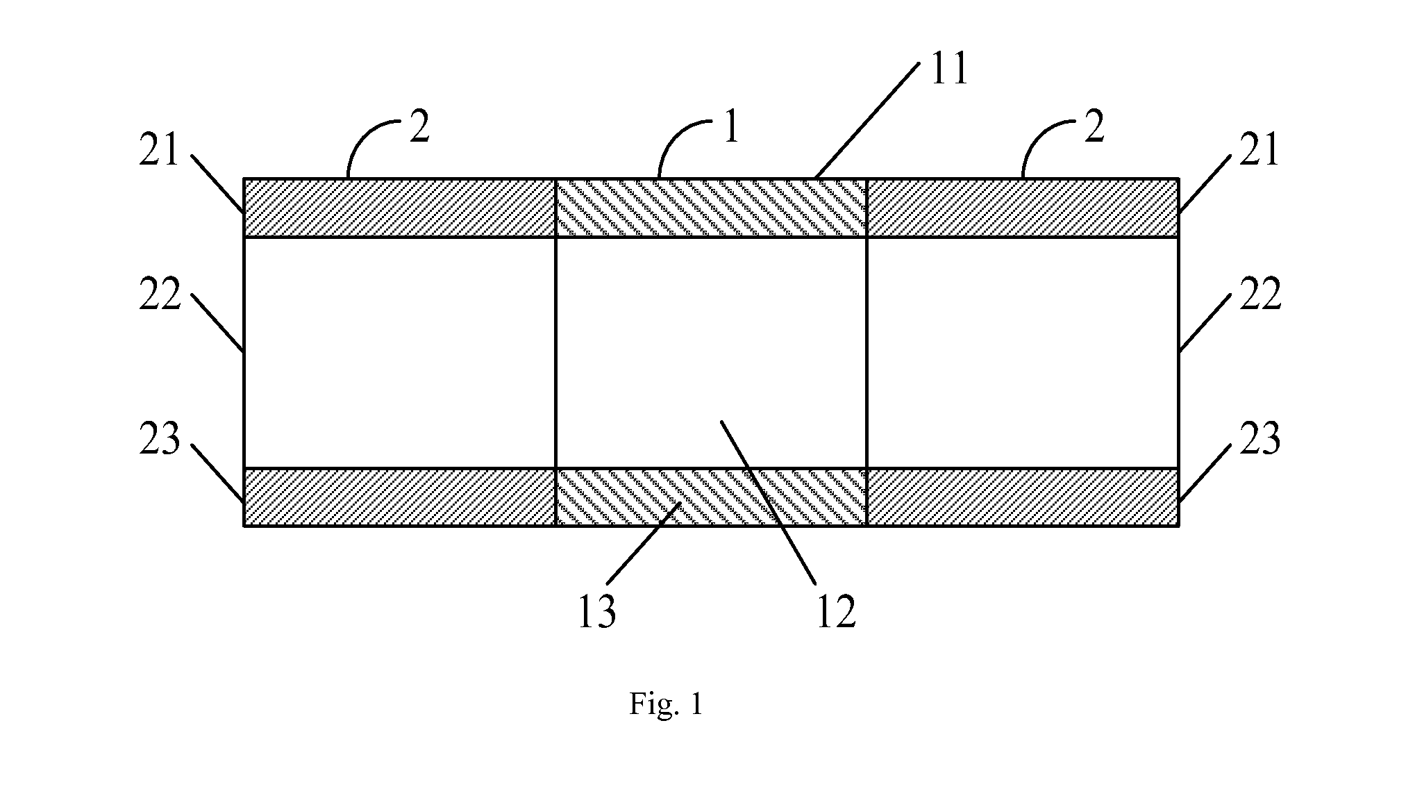
The present invention provides an LED chip packaging structure, manufacturing method, and display device that increase thermal conductivity and overall stability, and improve light-extraction effect of the LED chip surface. The LED chip and the conductive unit are connected without using welding gold wire, which reduces the overall thickness of the LED chip device and enhances the thermal conductivity of the LED chip. The LED chip surface is improved by forming a conductive layer and an intermediate isolation layer, which facilitate the flow of electric current and reduce the loss of light.

Problems solved by technology

As a result, a large resistance and a large quantity of heat will occur.
Because the electrode and gold wire welded on a light-extraction surface of the LED chip will prevent a portion of light from passing therethrough, the LED chip will have low light extraction efficiency and poor light extraction consistency.
In addition, sophisticated instruments and complex processes are required for welding the gold wire, so the operation process is complicated and the cost is high.

Method used


Image

  • LED chip packaging structure, its manufacturing method, and display device
  • LED chip packaging structure, its manufacturing method, and display device
  • LED chip packaging structure, its manufacturing method, and display device

Examples


Embodiment Construction

[0048]To make the objects, the technical solutions and the advantages of the embodiments of the present invention more apparent, the embodiments of the present invention will be described clearly and completely hereinafter in conjunction with the drawings. Obviously, the followings are merely a part of, rather all of, the embodiments of the present invention. Based on the following embodiments, all the other embodiments obtained by a person skilled in the art without any creative effort also fall in the scope of the present invention.

[0049]Unless otherwise defined, all the terms (including technical and scientific terms) used herein have the same meaning as commonly understood by one of ordinary skill in the art to which this invention belongs. The terms “first”, “second” and the like used in the specification and claims are intended to differentiate different components, rather than to show the order, number or importance. Also, the terms “one”, “one of” and the like are intended t...


PUM


Abstract

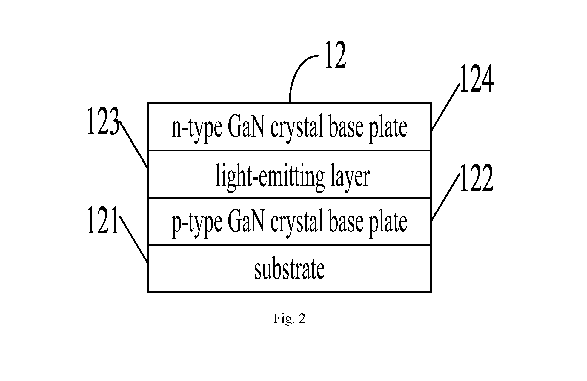
A LED chip packaging structure, its manufacturing method, and a display device are disclosed. A conductive unit is formed at two opposite sides of a LED chip unit, and comprises a first conductive layer formed at a side of, and electrically connected to, a first electrode, a second conductive layer formed at a side of, and electrically connected to, a second electrode, and an intermediate isolation layer formed at a side of a GaN layer. The LED chip unit and the conductive unit are connected laterally to form an electrical-connection channel as a whole, without welding a gold wire for the conductive channel as in a traditional LED. Thus, the method is able to reduce the total thickness of the LED chip device, increase the thermal conductivity effect of the LED chip and the overall stability, and improve the light-extraction effect of the surface of the LED chip.

Description

CROSS-REFERENCE TO RELEVANT APPLICATION[0001]The present application claims a priority of the Chinese patent application No. 201210545538.1 filed on Dec. 14, 2012, which is incorporated herein by reference in its entirety.TECHNICAL FIELD[0002]The embodiments of the present invention relate to the field of LED packaging technology, in particular to a LED chip packaging structure, its manufacturing method and a display device.BACKGROUND[0003]The occurrence of semiconductor light-emitting diode (LED) leads to a reform of the lighting industry once again. Due to the advantages such as miniaturization and solidification, vibration resistance, fast instant startup, rapid response, energy-saving, long service life and environmental efficiency, the LED has been widely used in general lighting, backlight units and decorative lighting. The high-power and high-brightness LEDs have a great prospect in replacing incandescent lamps.[0004]In industry, one way of producing white light is to coat a ...

Claims


Application Information

Patent Timeline
IPC IPC(8): H01L33/22H01L23/00H01L33/32H01L33/62H01L33/64
CPCH01L33/32H01L33/62H01L33/647H01L24/95H01L2933/0066H01L2933/0075H01L2924/12041H01L2924/12042H01L25/0753H01L33/007H01L33/0075H01L2924/00
Inventor ZHENG, WEIXINMA, GUOHENGYANG, DONGSHENGQIAO, ZHONGLIAN
Owner BOE TECH GRP CO LTD
Learn More