
Organic light-emitting device and preparation method thereof

An electroluminescent device and luminescent technology, applied in the field of OLED devices, can solve problems such as inability to completely eliminate short-circuit points, lower device efficiency, and OLED screen failure, so as to avoid material decomposition and breakdown problems, prevent leakage current and device Effect of failure, elimination of plasma mode loss

Active Publication Date: 2021-03-30
GUAN YEOLIGHT TECH CO LTD
View PDF10 Cites 1 Cited by
  • Summary
  • Abstract
  • Description
  • Claims
  • Application Information

AI Technical Summary

Problems solved by technology

[0002] OLED screens are widely used for their ultra-thin, large-area uniformity, and excellent heat dissipation. Because the total thickness of the organic layer of OLED devices is on the order of tens to hundreds of nanometers, the distance between the OLED anode and cathode is particularly small. In the process of OLED screen preparation, defect points such as dust particles, burrs, pinholes, and cracks in the surrounding environment will inevitably adhere to each layer of the OLED. The defect points will cause direct contact between the anode and the cathode, resulting in a short circuit. The current flows through the short-circuit point, generating a large amount of heat to cause the OLED screen to fail in the form of burning, ablation, and rupture.
[0003] The existing anti-short-circuit technology mainly has two methods. One is to cover defect points by increasing the thickness of the organic layer, but this method requires OLED devices to use higher driving voltages, resulting in lower device efficiency. The method cannot completely eliminate the short-circuit point, and dust particles will be generated during the thickening evaporation process, because the size of the defect varies from nanometer to micron, this method cannot completely solve it, and can only cover part of the defect point effect
Another way is to use structure or material to make the anti-short circuit part. For example, in the Chinese patent document CN105103330B, the conductive connection unit and the first electrode current-carrying unit or auxiliary electrode are used. Although this method effectively improves reliability, the short-circuit prevention part Existence will lead to a decrease in the aperture ratio of the device, which also indirectly reduces the efficiency of the device

Method used


Image

  • Organic light-emitting device and preparation method thereof
  • Organic light-emitting device and preparation method thereof
  • Organic light-emitting device and preparation method thereof

Examples


Embodiment 1

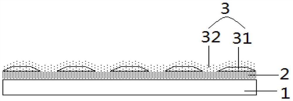
[0044] like Figure 1-5 As shown, the present invention provides an organic electroluminescent device, comprising a substrate 1, a transparent electrode layer 2, an organic functional layer 4 and a metal cathode layer 6 disposed on the transparent electrode layer 2, the transparent electrode layer 2 and the organic functional layer The undulating transparent resistance layer 3 is arranged between the 4, and the surface of the organic functional layer 4 is arranged on the undulating transparent resistance layer 3 in an undulating shape. By designing the transparent resistance layer on the transparent electrode layer, the surface of the transparent resistance layer is undulating, and the accompanying fluctuations of the organic functional layer 4 and the reflective metal cathode layer 6 eliminate the plasma on the flat surface of the metal cathode layer 6 to a certain extent. Mode loss; at the same time, the existence of the transparent resistance layer eliminates the short circ...

Embodiment 2

[0062] like Figure 2-5 As shown, the present invention also provides a short-circuit proof light-emitting device with a light extraction structure, including a substrate 1, a transparent electrode layer 2, an organic functional layer 4 and a metal cathode layer 6 disposed on the transparent electrode layer 2, and the transparent electrode layer An undulating transparent resistive layer 3 is arranged between 2 and the organic functional layer 4, and the surface of the organic functional layer 4 is undulatingly arranged on the undulating transparent resistive layer 3. like image 3 As shown, a grid or porous structure a is formed on the surface of the transparent electrode layer 2. The grid or porous structure a in the figure is a circular hole with the same or different upper and lower diameters, and its maximum aperture is 5 μm-500 μm. For polygonal holes such as triangular holes and square holes with the same or different calibers, the longest distance between two points co...

Embodiment 3

[0086] On the basis of Embodiment 2, this embodiment etches the grid or porous structure formed on the surface of the transparent electrode 2, and etches such as Figure 2-5 The indicated taper angles (inclination angles) β are 10°, 20°, 30°, 40°, 50°, 60°, 70°, and 80° respectively. The following table shows the performance comparison of the corresponding angles.

[0087]

[0088]

[0089] It can be seen from the comparison that different taper angles β have different light extraction efficiencies. When the taper angle β is 30°-60°, the device in the above table generates the smallest passing current and the highest brightness. This is because the taper angle β is greater than 60° When the taper angle β is less than 30°, the direction of the light and the morphology of the cathode cannot be effectively changed due to the inconspicuous undulation. Of course, the relief layer formed in the present invention can also be caused by the relief of the metal layer grid or other...


PUM

PropertyMeasurementUnit
thicknessaaaaaaaaaa
thicknessaaaaaaaaaa
thicknessaaaaaaaaaa

Abstract

The invention discloses an organic light-emitting device and a preparation method thereof, the organic light-emitting device comprises a transparent electrode layer, an organic functional layer and ametal cathode layer, the organic functional layer and the metal cathode layer are arranged on the transparent electrode layer, and an undulating transparent resistance layer is arranged between the transparent electrode layer and the organic functional layer. And the surface of the organic functional layer is arranged on the undulating transparent resistance layer in an undulating manner. According to the invention, the transparent resistance layer with the fluctuating structure is arranged between the transparent electrode layer and the organic functional layer, and along with the fluctuationof the organic functional layer and the reflection cathode layer, the plasma mode loss of the flat surface of the cathode metal is eliminated to a certain extent; by setting proper thickness, resistance value and light transmittance, the transparent resistance layer has the advantages of preventing short circuit failure of the screen body and improving light output efficiency.

Description

technical field [0001] The invention relates to the technical field of OLED devices, in particular to an organic electroluminescent device and a preparation method thereof. Background technique [0002] OLED screens are widely used for their ultra-thin, large-area uniformity, and excellent heat dissipation. Because the total thickness of the organic layer of OLED devices is on the order of tens to hundreds of nanometers, the distance between the OLED anode and cathode is particularly small. In the process of OLED screen preparation, defect points such as dust particles, burrs, pinholes, and cracks in the surrounding environment will inevitably adhere to each layer of the OLED. The defect points will cause direct contact between the anode and the cathode, resulting in a short circuit. All the current flows through the short-circuit point, generating a large amount of heat to cause the OLED screen to fail in the form of burning, ablation, and rupture. [0003] The existing an...

Claims


Application Information

Patent Timeline
Patent Type & Authority Applications(China)
IPC IPC(8): H01L51/52H01L51/56
CPCH10K50/85H10K50/86H10K71/00
Inventor 张国辉朱映光鲁天星董艳波胡永岚李栋栋苏乃文
Owner GUAN YEOLIGHT TECH CO LTD
Learn More