Image sensor and method for manufacturing the same

Active Publication Date: 2008-06-26
MARVELL ASIA PTE LTD
View PDF15 Cites 2 Cited by
  • Summary
  • Abstract
  • Description
  • Claims
  • Application Information

AI Technical Summary

Benefits of technology

[0008]Embodiments of the invention provide a method for manufacturing an

Problems solved by technology

Thereby, the light quantity incident on the microlens from outside the image sensor a

Method used


Image

  • Image sensor and method for manufacturing the same
  • Image sensor and method for manufacturing the same
  • Image sensor and method for manufacturing the same

Examples


Example

[0015]An image sensor and a method for manufacturing the same according to embodiments of the invention will be described with reference to the accompanying drawings.

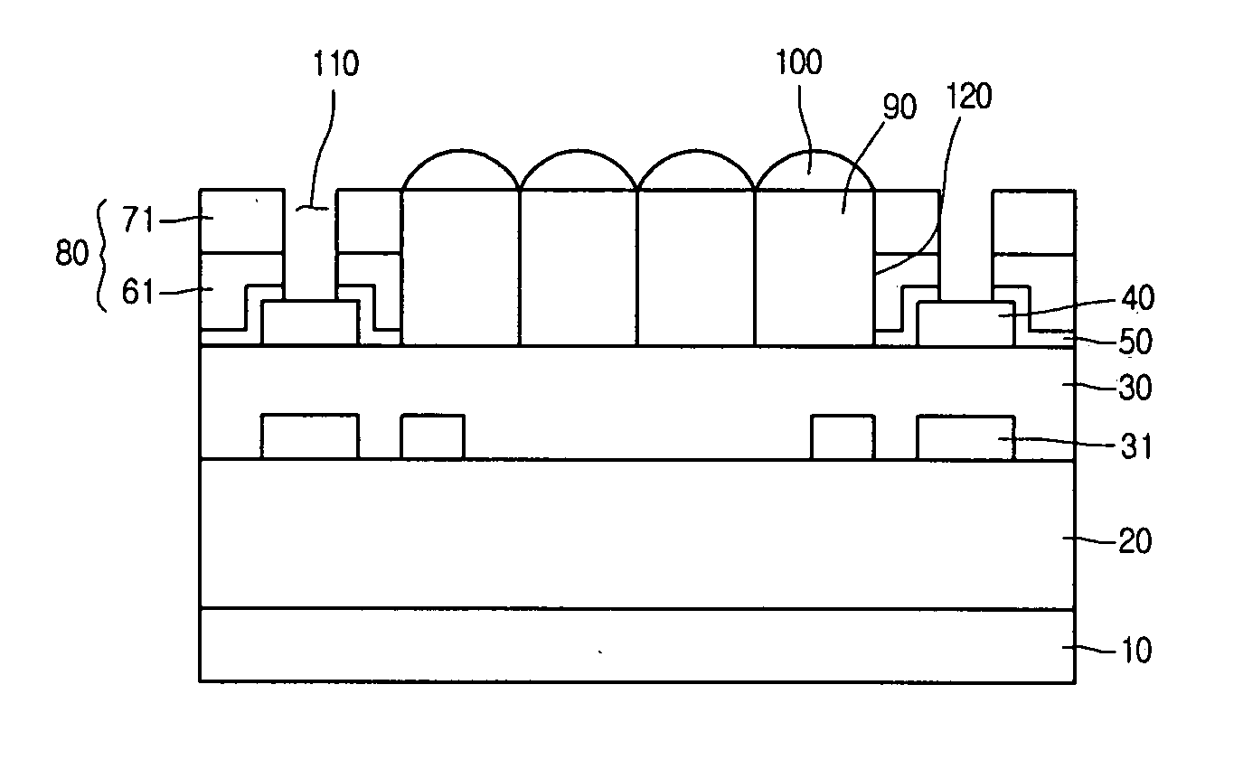
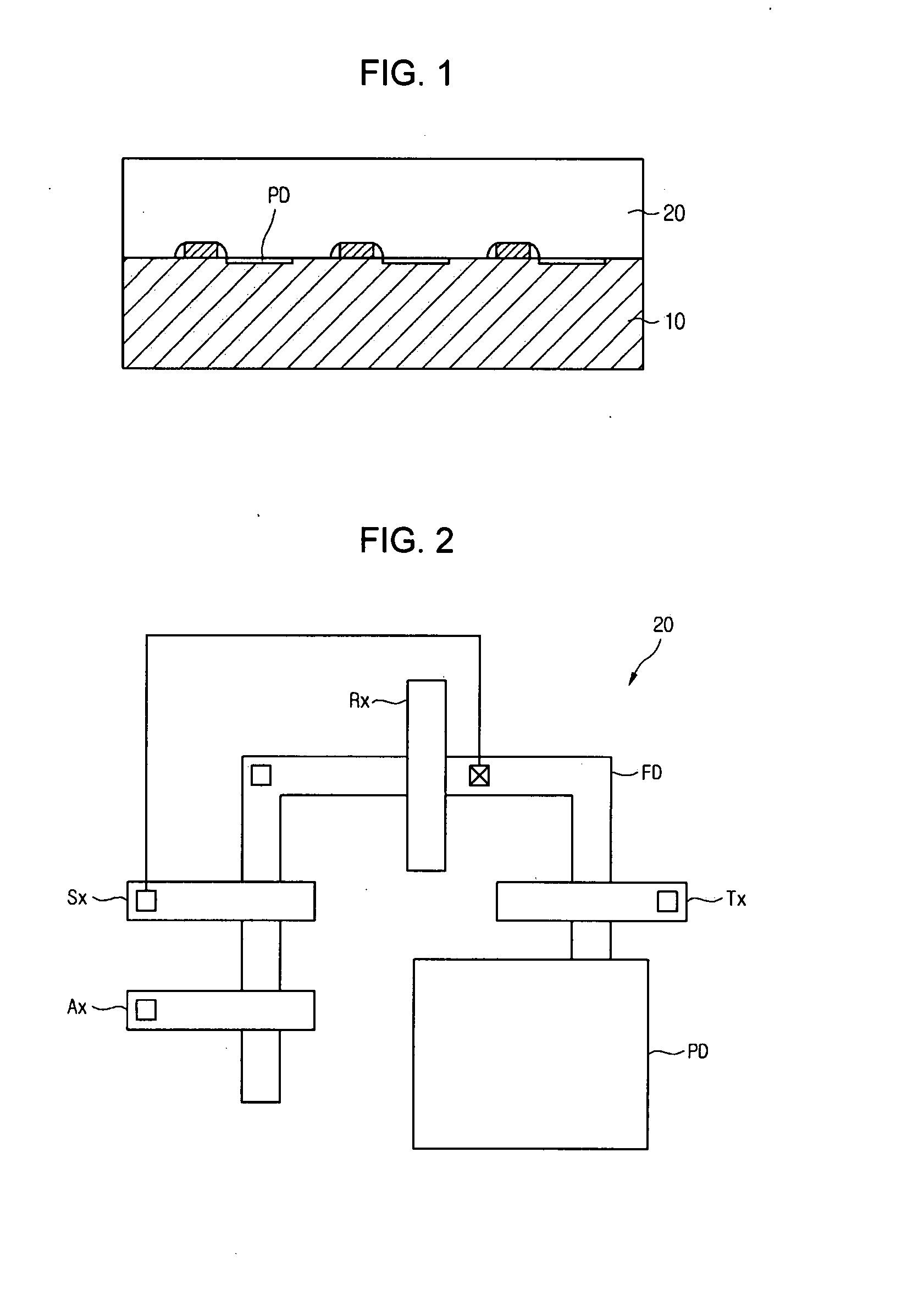
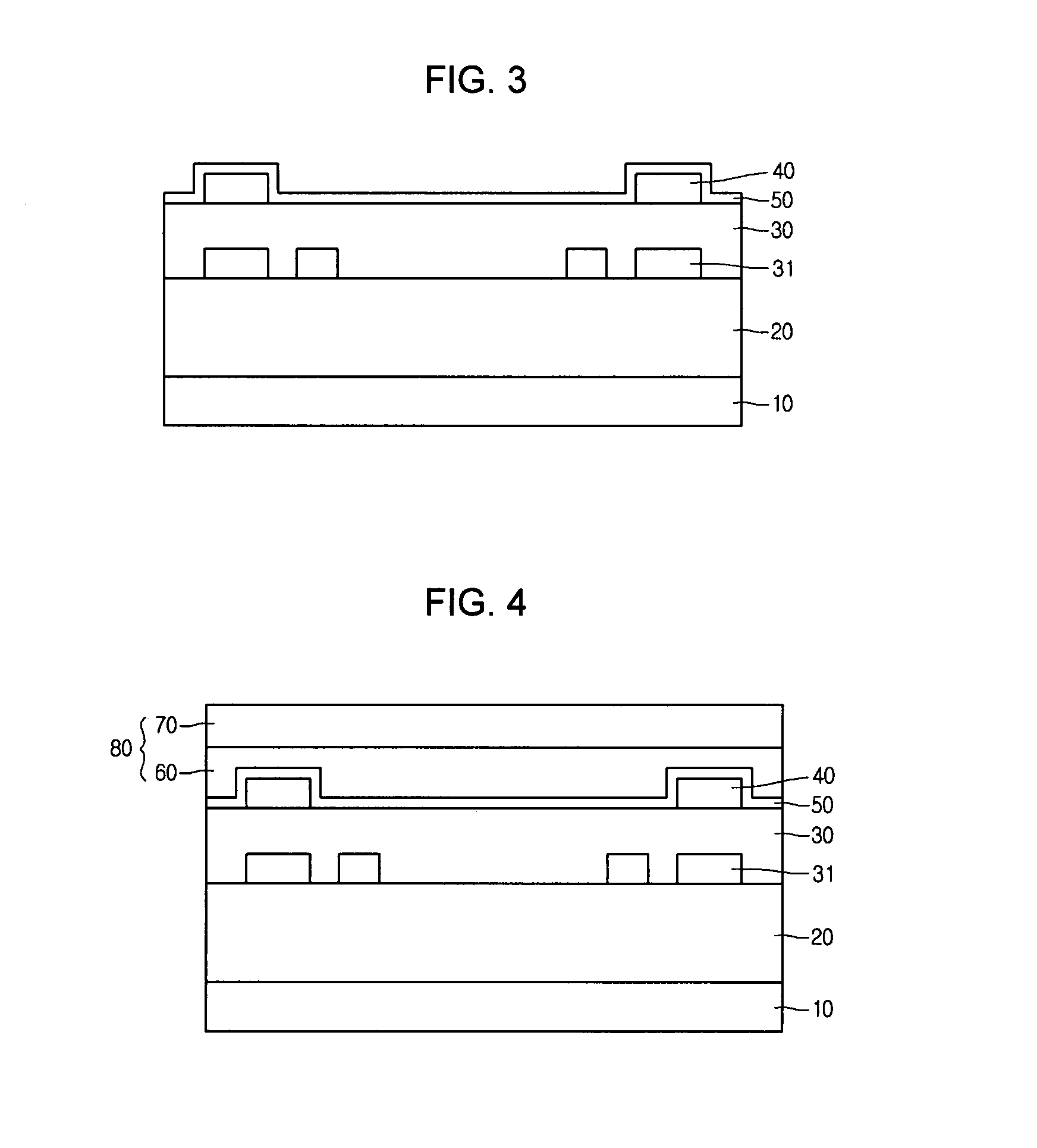
[0016]FIG. 7 is a cross-sectional view showing an exemplary image sensor according to embodiments of the invention. In the exemplary image sensor, a pixel array comprising a photodiode structure 20 and an insulating film structure 30 is formed on a semiconductor substrate 10. Herein, the exemplary image sensor has a structure where multiple pixels, each comprising a photodiode and a plurality of MOS transistors, are formed. The array of pixels may comprise an x-by-y array of rows and columns, where x and y are each independently an integer of at least 2, 3, 4, 8, 16, etc. The array may also comprise two or more blocks of pixels, each containing such an array. Typically, each unit pixel contains from 3 to 5 transistors.

[0017]Also, the insulating film structure 30 comprises an interlayer dielectric layer for insulation an...


PUM


Abstract

A method for manufacturing a sensor image may include forming a pixel array including a photodiode structure and an insulating film structure in an active area of a semiconductor substrate; forming a metal pad on the insulating film structure; forming a dielectric and/or etch stop film on the metal pad (and optionally over the pixel array); forming a protective layer on the dielectric and/or etch stop film; and forming a pad opening and a pixel opening by etching the protective layer.

Description

[0001]The present application claims priority under 35 U.S.C. 119 and 35 U.S.C. 365 to Korean Patent Application No. 10-2006-0131288 (filed on Dec. 20, 2006), which is hereby incorporated by reference in its entirety.BACKGROUND[0002]1. Field of the Invention[0003]The embodiment relates to an image sensor and a method for manufacturing the same.[0004]2. Description of the Related Art[0005]An image sensor, which is a semiconductor device converting an optical image into electrical signals, may be characterized as a charge coupled device (CCD) image sensor or a Complementary Metal Oxide Silicon (CMOS) image sensor. The CMOS image sensor includes a photodiode and MOS transistors in a unit pixel to sequentially produce and detect electrical signals in a switching manner, implementing an image. The CMOS image sensor includes transistors and a pixel arrays in which the photodiode is electrically connected to the transistors on a semiconductor substrate. An insulating film structure includi...

Claims


Application Information

Patent Timeline
IPC IPC(8): H01L31/00H01L21/02
CPCH01L27/14609H01L27/14687H01L27/14627H01L27/14621H01L27/146
Inventor IM, KI SIKHYUN, WOO SEOK
Owner MARVELL ASIA PTE LTD
Why Eureka
Try Eureka