Semiconductor Device

a technology of semiconductor devices and semiconductor components, applied in the direction of instruments, electrochemical variables, materials, etc., can solve the problems of wasting electric power supplied from outside, deterioration of the internal element of the semiconductor device, and deterioration of the semiconductor device itself, so as to reduce the number of components and reduce the cost , the effect of reducing the number of connections to the other circuit components

Active Publication Date: 2008-06-26
SEMICON ENERGY LAB CO LTD
View PDF31 Cites 44 Cited by
  • Summary
  • Abstract
  • Description
  • Claims
  • Application Information

AI Technical Summary

Benefits of technology

[0021]Further, by forming all of a plurality of circuits over the same substrate, the number of component parts can be reduced to reduce cost, and the number of connections to the other circuit components can be reduced to improve reliability. Alternatively, part of the circuits may be formed over a substrate and the other part of the circuits may be formed over another substrate. That is, not all of the circuits are required to be formed over the same substrate. For example, part of the circuits may be formed with transistors over a glass substrate, and the other part of the circuits may be formed using a single crystalline substrate and an IC chip thereof may be connected by COG (Chip On Glass) so as to be disposed over the glass substrate. Alternatively, the IC chip may be connected to the glass substrate by TAB (Tape Automated Bonding) or a printed wiring board. In this manner, by forming part of the circuits over the same substrate, for example, the number of component parts can be reduced to reduce cost, and the number of connections between the circuits and the component parts can be reduced to improve reliability. In addition, by forming a portion with a high driving voltage or a portion with high driving frequency over a different substrate, increase of power consumption can be prevented.
[0022]As a structure of a transistor usable for a data carrier, a multi-gate structure including two or more gates may be employed. With the multi-gate structure, off-current can be reduced, reliability can be improved by increasing the withstand voltage of the transistor, and a source-drain current is not changed so much even if a source-drain voltage is changed when operating in the saturation region so that flat characteristics can be achieved. Further, a structure in which gate electrodes are provided above and below a channel may also be employed. By employing the structure in which gate electrodes are provided above and below a channel, a channel region is increased, so that a current value can be increased and an S factor can be reduced because a depletion layer is easily formed. Further, any structure of the following may also be employed: a structure in which a gate electrode is disposed above a channel; a structure in which a gate electrode is disposed below a channel; a staggered structure; and an inversely staggered structure. A channel region may be divided into a plurality of regions, and the divided channel regions may be connected in parallel or in series. Further, a source or drain electrode may be overlapped with a channel region (or a part thereof). By employing the structure in which a source or drain electrode is overlapped with a channel region (or a part thereof), operational instability due to charge accumulation in part of a channel can be prevented. Further, an LDD region may also be provided in a source or drain region. By provision of an LDD region, off-current can be reduced, reliability can be improved by increasing the withstand voltage of the transistor, and a source-drain current is not changed so much even if a source-drain voltage is changed when operating in the saturation region so that flat characteristics can be achieved.
[0023]By using the present invention, even in the case where the communication distance is extremely short and a large amount of electric power is supplied to a semiconductor device, a defect which would occur in the semiconductor device is prevented, and electric power which is not needed for circuit operation of the semiconductor device (extra electric power) is not wasted but is stored in a battery, whereby effective use of electric power can be achieved.

Problems solved by technology

When a large amount of electric power is supplied to the semiconductor device, the semiconductor device cannot correctly demodulate a signal from the reader / writer and malfunctions, so that an internal element of the semiconductor device is deteriorated.
In the worst case, the semiconductor device itself could be destroyed.
In this case, however, electric power supplied from outside is wasted.

Method used


Image

  • Semiconductor Device
  • Semiconductor Device
  • Semiconductor Device

Examples


embodiment mode 1

[0047]In this embodiment mode, one example of a structure and operation of the semiconductor device of the present invention is described using drawings.

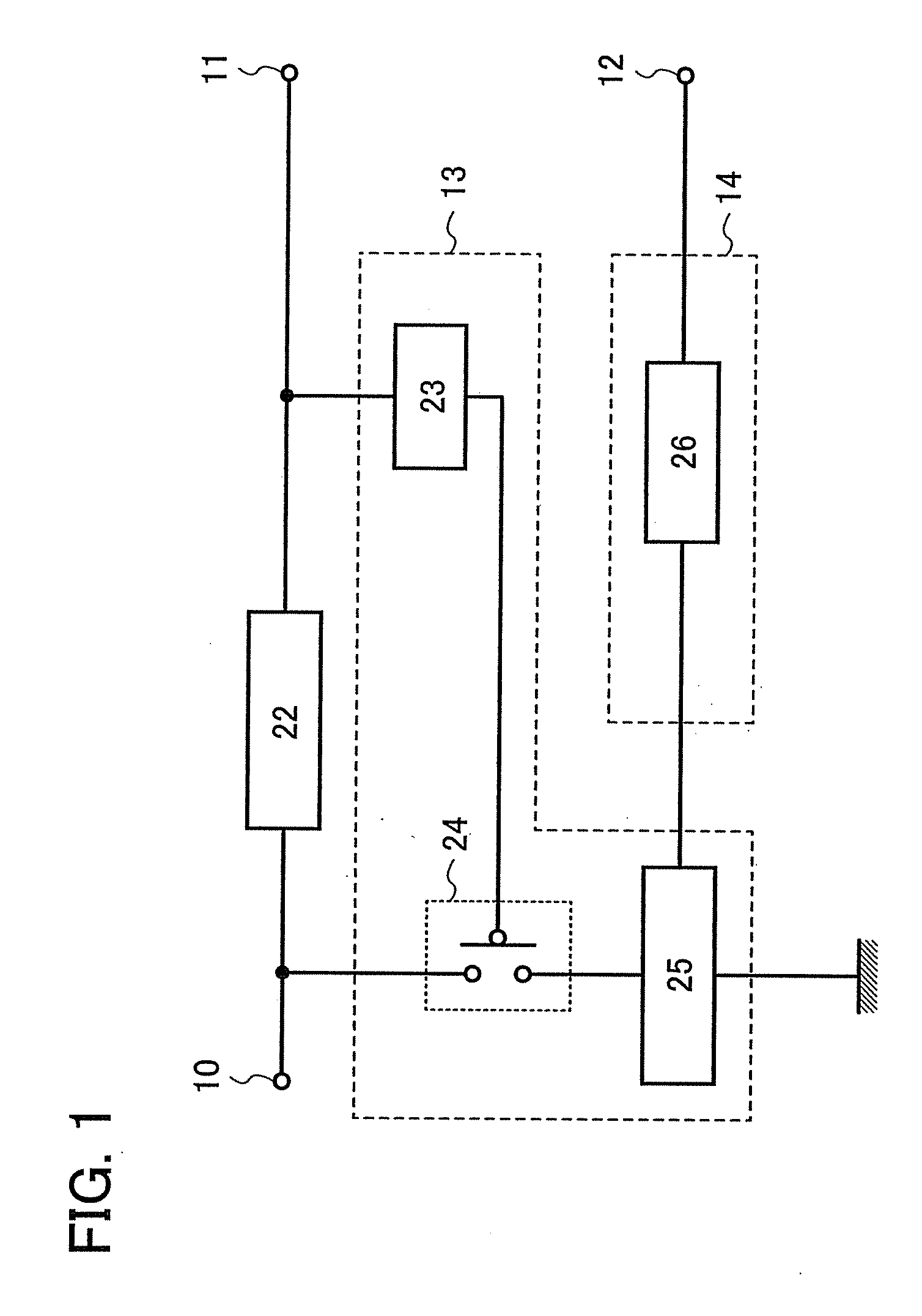
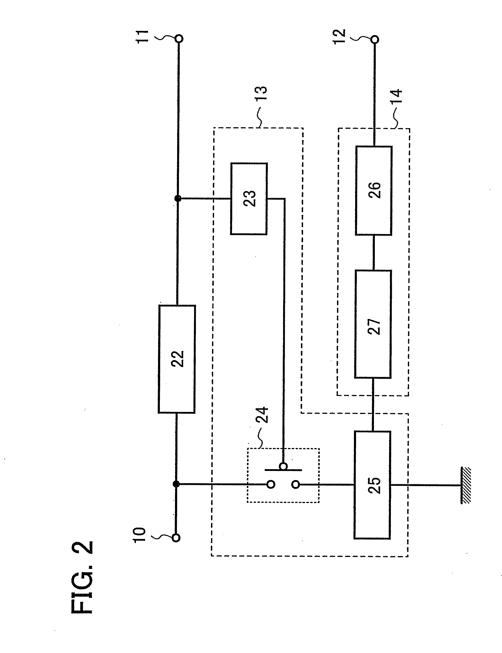
[0048]A semiconductor device described in this embodiment mode includes an input portion 10; a first DC converter circuit 22; a limiter circuit 13 including a first detecting circuit 23, a switching element 24, and a second DC converter circuit 25; and a charging circuit 14 including a battery 26 (see FIG. 1). A direct-current voltage, after being converted by the first DC converter circuit 22, is output to a first output portion 11, and electric power of the battery 26 is supplied to a circuit connected to an output portion 12.

[0049]The input portion 10 can, for example, be connected to an antenna, where electric power received by the antenna is supplied thereto.

[0050]The first DC converter circuit 22 converts an alternating-current voltage that is output from the input portion 10 into a direct-current voltage to be output to the f...

embodiment mode 2

[0076]In this embodiment mode, the case where the semiconductor device of the present invention is provided as a wireless tag (also called an RFID (Radio Frequency Identification) tag, an IC (Integrated Circuit) tag, an IC chip, an RF tag, or an electronic tag) which can communicate data wirelessly is described using drawings.

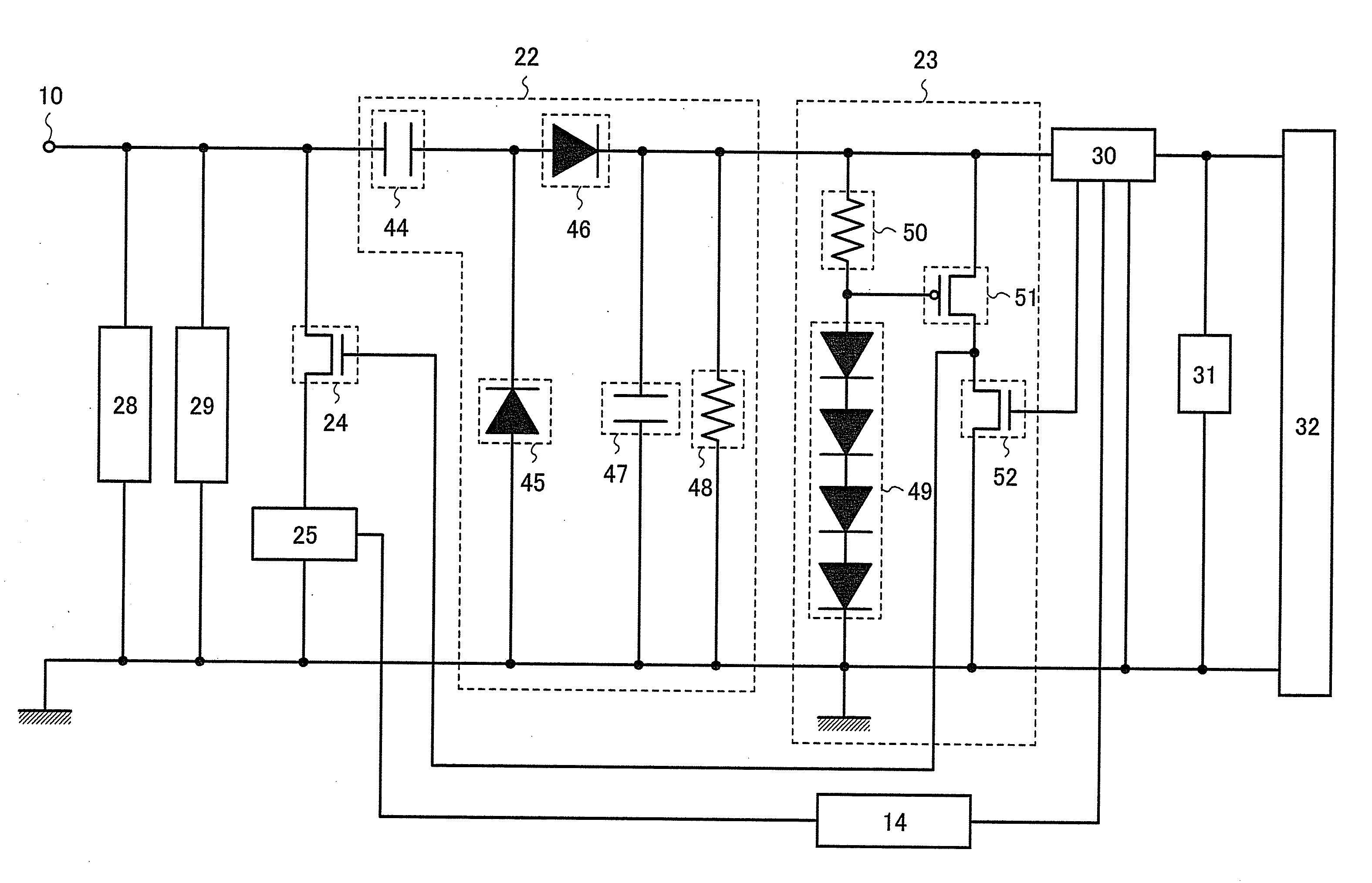
[0077]A semiconductor device described in this embodiment mode includes an antenna 40; the first DC converter circuit 22; the limiter circuit 13; the charging circuit 14; a modulating circuit 28 which modulates encoded data; a demodulating circuit 29 which digitalizes a signal received from the antenna 40; a constant voltage circuit 30 which makes an output voltage of the first DC converter circuit 22 a constant voltage; a clock generating circuit 31; an encoding circuit 32; a controller circuit 33; a judging circuit 34; and a memory 35 (see FIG. 3). Note that the limiter circuit 13 includes the first detecting circuit 23, the switching element 24, and the seco...

embodiment mode 3

[0096]A semiconductor device described in this embodiment mode includes the first DC converter circuit 22; the limiter circuit 13; the charging circuit 14; a first constant voltage circuit 54; a second constant voltage circuit 55; and a first discharge controller circuit 201. Note that the limiter circuit 13 includes the first detecting circuit 23, the switching element 24, and the second DC converter circuit 25, the charging circuit 14 includes the battery 26, and the first discharge controller circuit 201 includes a second detecting circuit 43, a switching element 56, a switching element 57, and the buffer 36 (see FIG. 6).

[0097]Operation of the semiconductor device described in this embodiment mode is described below. Note that, in the description hereinafter, when the first discharge controller circuit 201 does not operate, the switching element 56 is maintained at the ON state and the switching element 57 is maintained at the OFF state.

[0098]First, an alternating-current voltage...


PUM


Abstract

A semiconductor device which can operate normally even when the communication distance is extremely short, and which stores excess electric power which is not needed for circuit operation of the semiconductor device when a large amount of electric power is supplied thereto. The following are included: an antenna; a first AC/DC converter circuit which is connected to the antenna; a second AC/DC converter circuit which is connected to the antenna through a switching element; a detecting circuit which controls operation of the switching element in accordance with the value of a voltage output from the first AC/DC converter circuit; and a battery which stores electric power supplied from the antenna through the second AC/DC converter circuit. When the switching element is operated, electric power supplied from outside is at least partly supplied to the battery through the second AC/DC converter circuit.

Description

BACKGROUND OF THE INVENTION[0001]1. Field of the Invention[0002]The present invention relates to a semiconductor device which performs data communication (reception and transmission) by wireless communication. The present invention relates to, in particular, a semiconductor device including a protection circuit which prevents element deterioration or element destruction of the semiconductor device when a large amount of electric power is received by wireless communication.[0003]2. Description of the Related Art[0004]Nowadays, an individual identification technology using wireless communication (hereinafter referred to as a wireless communication system) has attracted attention. In particular, as a data carrier which communicates data by wireless communication, an individual identification technology with a semiconductor device utilizing an RFID (Radio Frequency Identification) technology (also called an RFID tag, an RF tag, an IC (Integrated Circuit) tag, an IC chip, a wireless tag,...

Claims


Application Information

Patent Timeline
Patent Type & Authority Applications(United States)
IPC IPC(8): H02J7/00
CPCH02J17/00H02J7/022H02J50/001H02J2207/20H02J50/10H02J50/005
Inventor KATO, KIYOSHIFURUTANI, KAZUMA
Owner SEMICON ENERGY LAB CO LTD
Why Eureka
Try Eureka