Drive Circuit and Drive Method for Liquid Crystal Display Device

a liquid crystal display device and drive circuit technology, applied in the direction of instruments, computing, electric digital data processing, etc., can solve the problems of unintended black screen and white screen, and achieve the effects of preventing the malfunction of the drive circuit of the scanning signal line, reducing the fluctuation of the electric potential of the power source, and preventing display problems

Active Publication Date: 2008-06-26
SHARP KK
View PDF6 Cites 13 Cited by
  • Summary
  • Abstract
  • Description
  • Claims
  • Application Information

AI Technical Summary

Benefits of technology

[0042]According to the first or the ninth aspect of the present invention, when starting display in a liquid crystal display device, all of the scanning signal lines are selected to release electric charges which are accumulated at capacities in each pixel formation portion, and thereafter, the scanning signal lines which have been in the Selected state are deselected in a stepwise manner. After deselecting all of the scanning signal lines in this way, sequential selection of the scanning signal lines for display, i.e. scanning, is started. Therefore, unlike in conventions where the scanning signal lines which have been in the Selected state are brought simultaneously to the Deselected state, the number of scanning signal lines in which the applied voltage changes simultaneously for the transfer from the Selected state to the Deselected state is remarkably smaller. This eliminates chances for an excessive current to pass through the bulk (silicon substrate) which constitutes the scanning signal line drive circuit, and therefore, there is reduced power source electric potential fluctuation caused by the current which flows through the bulk in the scanning signal line drive circuit when deselecting the scanning signal lines. As a result, it becomes possible to prevent malfunctions of the scanning signal line drive circuit caused by latch-ups for example, during a sequence of operations for electric potential discharge, i.e. the Display-ON sequence, performed for preventing display problems when starting the liquid crystal display device.
[0043]According to the second or the tenth aspect of the present invention, a plurality of scanning signal line groups created by grouping the scanning signal lines in the liquid crystal display device are deselected, one group at a time, in a stepwise manner; therefore, the selection-canceling section can be implemented with a simple configuration.
[0044]According to the third aspect of the present invention, the scanning signal lines are deselected in a stepwise manner, in a plurality of cycles at an interval of one horizontal scanning period, whereby it becomes possible to reduce power source electric potential fluctuation caused by the curren...

Problems solved by technology

Now, there is a problem known with such a liquid crystal display device as the above: When the liquid crystal display device is started and before forming an image on the pixel formation portions by sequentially selecting the scanning signal lines (i.e. before starting display), electric potential in the common electrode Ec and the ...

Method used


Image

  • Drive Circuit and Drive Method for Liquid Crystal Display Device
  • Drive Circuit and Drive Method for Liquid Crystal Display Device
  • Drive Circuit and Drive Method for Liquid Crystal Display Device

Examples


first embodiment

1. FIRST EMBODIMENT

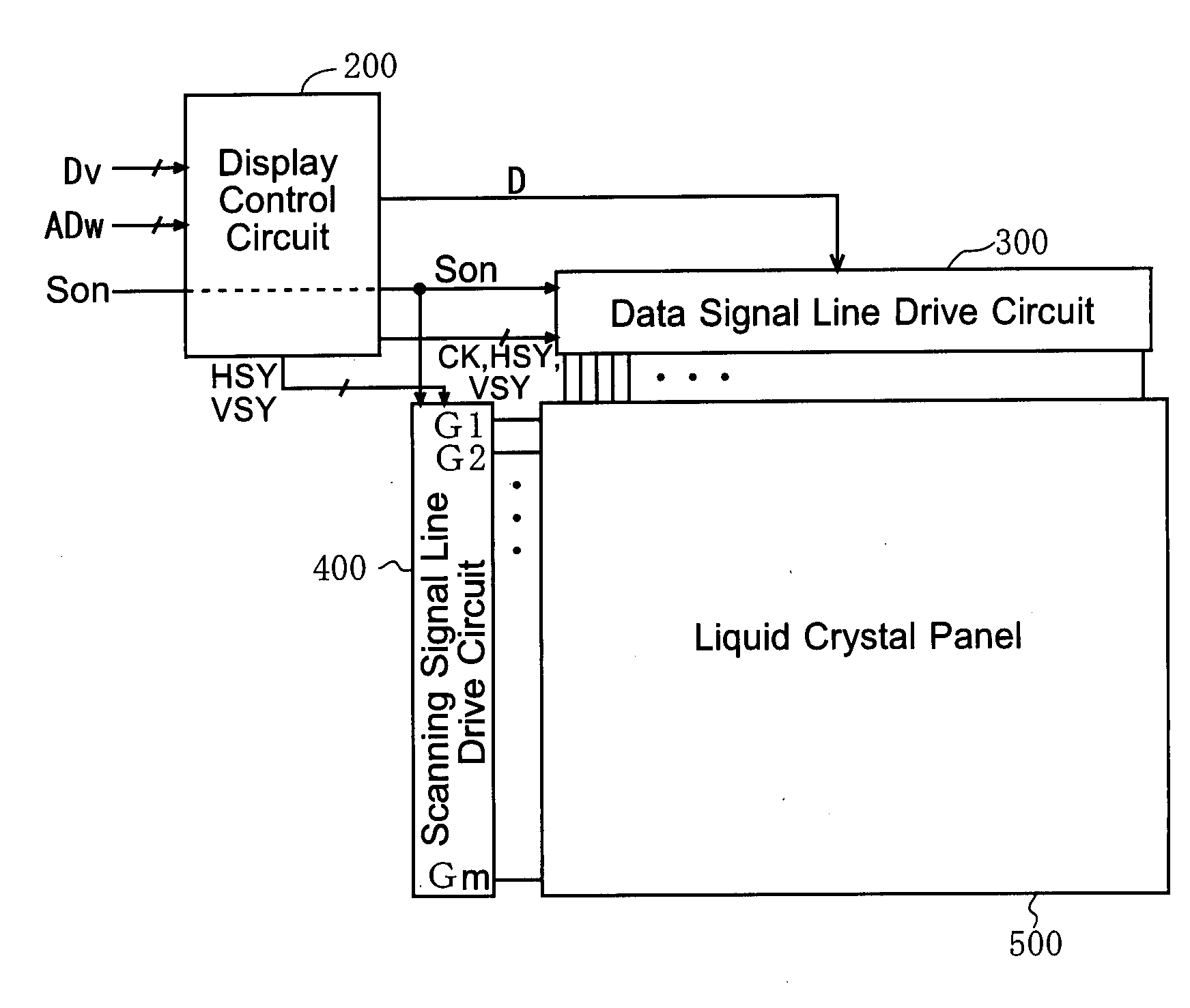
[0094]FIG. 1 is a block diagram which shows a configuration of a liquid crystal display device according to a first embodiment of the present invention. The liquid crystal display device includes: a display control circuit 200; a drive circuit constituted by a data signal line drive circuit 300 and a scanning signal line drive circuit 400; and an active matrix liquid crystal panel 500.

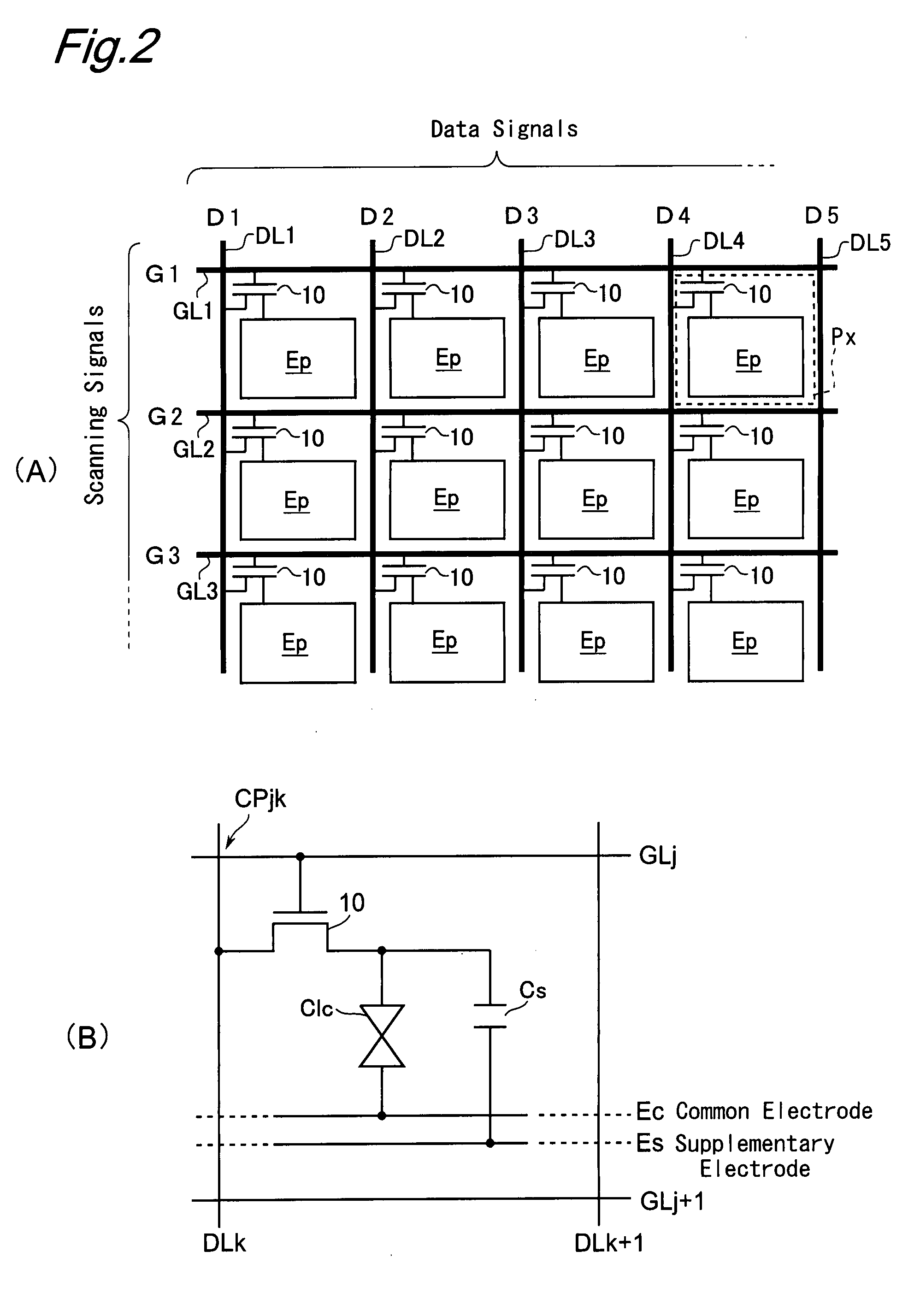
[0095]The liquid crystal panel 500, which serves as a display section in the liquid crystal display device, includes a plurality of scanning signal lines, a plurality of data signal lines crossing each of the scanning signal lines, and a plurality of pixel formation portions each provided correspondingly to one of the intersections made by the scanning signal lines and the data signal lines. Each of the scanning signal lines corresponds to one horizontal scan of an image data Dv received from e.g. an external CPU or other control section of an electronic appliance which uses the liqu...

second embodiment

2. SECOND EMBODIMENT

[0117]Next, a liquid crystal display device according to a second embodiment of the present invention will be described. The liquid crystal display device has essentially the same overall configuration as of the first embodiment, but uses a different operational method and scanning signal line drive circuit configuration therefor for deselecting the scanning signal lines which are once selected, in the Display-ON sequence. Hereinafter, description will focus mainly on these differences from the first embodiment. It should be noted that those components and elements in the liquid crystal display device in the second embodiment which are identical with or corresponding to those in the first embodiment will be indicated by the same alphanumerical symbols.

[0118]FIG. 6 shows waveform charts of the vertical synchronizing signal VSY, the gate OFF voltage VGL, the gate ON voltage VGH, the scanning signals (including the first-area through the fourth-area scanning signals...

third embodiment

3. THIRD EMBODIMENT

[0128]In the first and the second embodiments, the scanning signal line drive circuit 400 has a configuration shown in FIG. 5 or FIG. 7, where the flip-flops in the shift register 35 are reset in a stepwise manner by the reset signals R1-R4 in order to deselect the scanning signal lines, which have been brought to Selected state, in the Display-ON sequence. In place of this arrangement, stepwise deselection of the scanning signal lines may be achieved by changing a start pulse signal which is to be inputted to the shift register. Hereinafter, description will cover a third embodiment which includes a liquid crystal display device provided with such a scanning signal line drive circuit. Note that all of the aspects other than the scanning signal line drive circuit are identical with those in the first embodiment, so identical or corresponding components and elements are indicated by the same alphanumerical symbols, and no more description will be made here.

[0129]FI...


PUM


Abstract

A display ON sequence for preventing problems in a display at the starting time of a liquid crystal display device is prevented from having malfunctions, which might otherwise be caused in a scanning line drive circuit by applying a voltage to scanning signal lines. In the display ON sequence at the starting time of the liquid crystal display device of an active matrix type, all the scanning signal lines of a liquid crystal panel are brought into a selected state thereby to release the electric charges in the liquid crystal capacity and the auxiliary capacity in each pixel forming portion through data signal lines. After this, the scanning signal lines are stepwise brought into an unselected state by dividing them several times, before their sequential selections (or scans) for the display are started. Thus, the electric current to flow through the bulk of the scanning signal line drive circuit is made lower than that of the prior art, in which the scanning signal lines were simultaneously brought into the unselected state.

Description

TECHNICAL FIELD [0001]The present invention relates to drive circuits and drive methods for active matrix crystal display devices, and more specifically, to drive circuits and methods for discharging electric charges accumulated in pixel capacities in an active matrix liquid crystal display device when the device is started.BACKGROUND ART [0002]Conventional active matrix liquid crystal panels are constituted by two transparent substrates sandwiching a liquid crystal layer. One of the substrates is formed with a plurality of data signal lines (hereinafter may also called “source lines”) and a plurality of scanning signal lines (hereinafter may also called “gate lines”) crossing the data signal lines so as to provide a matrix of pixel formation portions each formed at one of the intersections. Each pixel formation portion includes a pixel electrode connected with one of the data signal lines that passes a corresponding intersection, via a TFT (Thin Film Transistor) which serves as a s...

Claims


Application Information

Patent Timeline
IPC IPC(8): G09G5/00
CPCG09G3/3648G09G2310/0205G09G2330/08G09G2330/026G09G2330/025
Inventor TAKAHASHI, KOZO
Owner SHARP KK
Why Eureka
Try Eureka