Supercharge Your Innovation With Domain-Expert AI Agents!

Method for cleaning silicon wafer

a technology for cleaning silicon wafers and silicon wafers, applied in the preparation of detergent mixture compositions, cleaning using liquids, inorganic non-surface active detergent compositions, etc., can solve the problems of reducing the production yield of semiconductor devices, contaminated silicon wafer surfaces, and increasing semiconductor device production costs

Inactive Publication Date: 2008-07-03
LG SILTRON
View PDF3 Cites 4 Cited by
  • Summary
  • Abstract
  • Description
  • Claims
  • Application Information

AI Technical Summary

Problems solved by technology

Surfaces of silicon wafers are contaminated by various impurities during a wafer fabricating process or a semiconductor process for device integration.
Such impurities cause the reduced production yield of semiconductor devices.
As a result, production costs of semiconductor devices are increased, and considerable costs are spent in treating a large quantity of chemical materials emitted in the cleaning processes.
However, the typical SC-1 cleaning solution causes metal induced pits (called ‘MIPs’ for short) occurring when etching the surfaces of a silicon substrate or removing the metallic impurities from the surfaces of the silicon substrate, so that the surfaces of the silicon substrate may become rough.
As a result, the typical SC-1 cleaning solution infavorably reduces an electrical characteristic of an insulating layer formed on the silicon substrate.
The technique advantageously makes the surfaces of the silicon wafer clean, however, in the case that plenty of impurities such as metallic ions exist on the surfaces of the silicon wafer, a single-time cleaning process according to the technique may be insufficient to completely remove the impurities and the removed metallic impurities may be attached to the silicon wafer again.
Thus, disadvantageously the technique should repeat the cleaning process for improved cleaning effect.
In this case, however, an excessive amount of cleaning solution is used, so that a dehydrogenation process should be performed when treating waste water after the cleaning processes and process costs are increased.
Further, the cleaning processes should be performed at high temperature, so that much energy is consumed, and a portion of the metallic impurities removed by the cleaning processes is attached to the silicon wafer again and acts as contamination.

Method used


Image

  • Method for cleaning silicon wafer
  • Method for cleaning silicon wafer
  • Method for cleaning silicon wafer

Examples


Embodiment Construction

[0020]Hereinafter, preferred embodiments of the present invention will be described in detail with reference to the accompanying drawings.

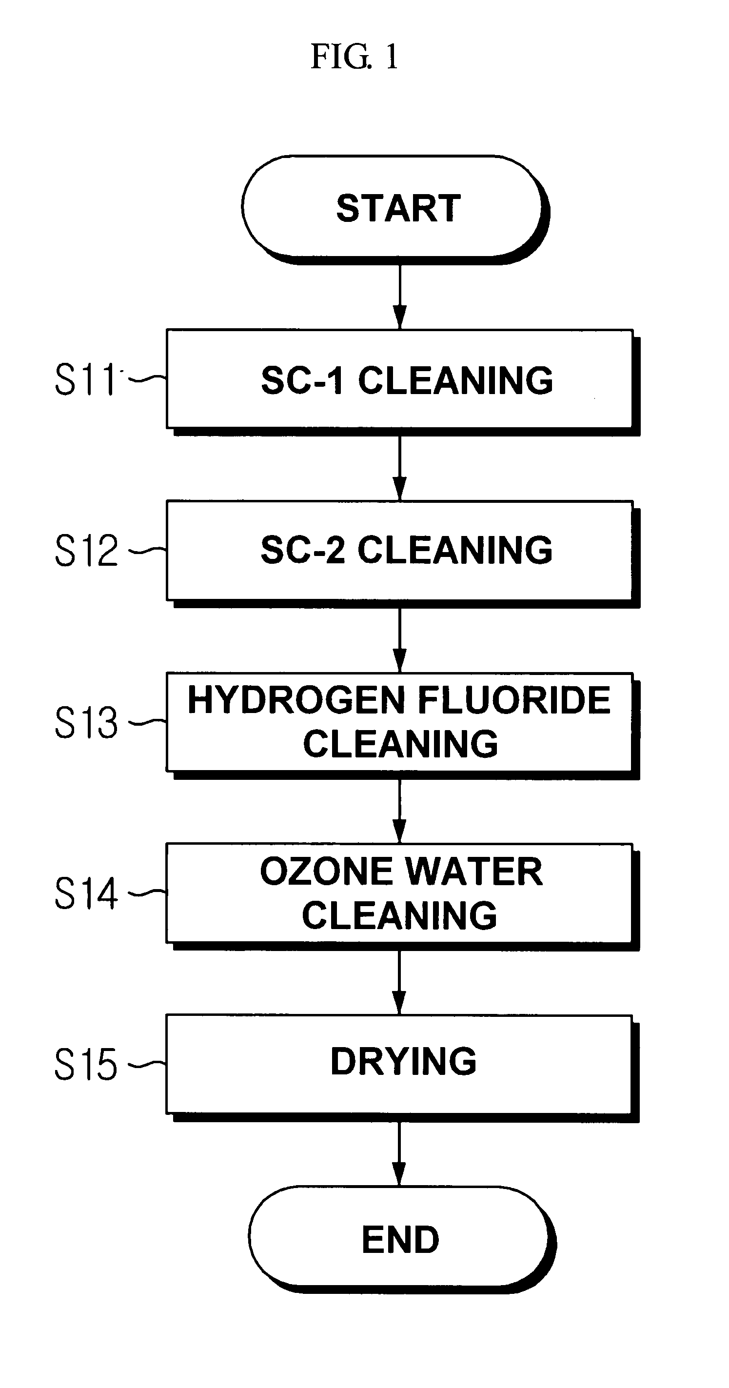
[0021]FIG. 1 is a flow chart illustrating a method for cleaning a silicon wafer according to the present invention.

[0022]Referring to FIG. 1, an entire cleaning process consists of four steps: (S11) a first step for cleaning using an SC-1 cleaning solution; (S12) a second step for cleaning using an SC-2 cleaning solution; (S13) a third step for cleaning using a hydrogen fluoride (HF) solution; (S14) a fourth step for cleaning using an ozone water; and (S15) a fifth step for drying the cleaned silicon wafer.

[0023]During a sequential progress of the steps (S11) to (S14), each step commonly includes removing the cleaning solution, used in the previous step and remaining on the surfaces of the silicon wafer, using DI (deionized) water.

[0024]The step (S11) is performed using the SC-1 cleaning solution that is a mixed solution of ammonia water and hydro...


PUM

PropertyMeasurementUnit
Temperatureaaaaaaaaaa
Fractionaaaaaaaaaa
Fractionaaaaaaaaaa

Abstract

The present invention relates to a method for cleaning a silicon wafer, including (S1) a first cleaning step for cleaning surfaces of a silicon wafer using an SC-1 cleaning solution according to standard clean 1; (S2) a second cleaning step for cleaning the surfaces of the silicon wafer, cleaned in the first cleaning step, using an SC-2 cleaning solution according to standard clean 2; (S3) a third cleaning step for cleaning the surfaces of the silicon wafer, cleaned in the second cleaning step, using a hydrogen fluoride (HF) solution; and (S4) a fourth cleaning step for cleaning the surfaces of the silicon wafer, cleaned in the third cleaning step, using an ozone water. The present invention removes effectively metallic impurities on the surfaces of the silicon wafer and improves the surface roughness of the silicon wafer, and thus is capable of providing a silicon wafer with a remarkably improved physical characteristic.

Description

BACKGROUND OF THE INVENTION[0001]1. Field of the Invention[0002]The present invention relates to a method for cleaning a silicon wafer, and in particular, to a method for cleaning a silicon wafer, in which cleaning processes are performed according to standard clean 1 and 2 and subsequently followed by additional cleaning processes using a hydrogen fluoride and an ozone water.[0003]2. Description of the Related Art[0004]Surfaces of silicon wafers are contaminated by various impurities during a wafer fabricating process or a semiconductor process for device integration. Typically, the impurities include fine particles, organic impurities or metallic impurities. Such impurities cause the reduced production yield of semiconductor devices. Therefore, when fabricating bare silicon wafers, a cleaning process should be performed after a polishing processing using CMP (Chemical Mechanical Polishing) and after a unit semiconductor process that generates much impurities, so that the concentra...

Claims


Application Information

Patent Timeline
IPC IPC(8): B08B3/08
CPCC11D7/08H01L21/02052C11D11/0047C11D2111/22H01L21/304
Inventor KIM, IN-JUNGBAE, SO-IK
Owner LG SILTRON
Features
  • R&D
  • Intellectual Property
  • Life Sciences
  • Materials
  • Tech Scout
  • Unparalleled Data Quality
  • Higher Quality Content
  • 60% Fewer Hallucinations
Learn More