Stressed barrier plug slot contact structure for transistor performance enhancement

a contact structure and barrier plug technology, applied in the field of new contact structures, can solve the problems of increasing the cost of these new tools and materials, increasing the cost of reducing the cost of reducing the cost of reducing the cost of reducing the cost of reducing the cost of reducing the cost of reducing the cost of reducing the cost of reducing the cost of reducing the cost of reducing the cost of reducing the cost of reducing the cost of reducing the cost of reducing the cost of reducing

Active Publication Date: 2008-07-03
INTEL CORP
View PDF16 Cites 196 Cited by
  • Summary
  • Abstract
  • Description
  • Claims
  • Application Information

AI Technical Summary

Problems solved by technology

However, as CMOS device size progresses further into the nano-sized regime, the associated cost of these new tools and materials can be prohibitive.
And in addition to economic constraints, scaling is also quickly approaching constraints of device materials and design.
Fundamental physical limits such as gate oxide leakage and source / drain extension resistance make continued minimization difficult to maintain.
However, silicon-germanium virtual substrates are costly to manufacture.
Accordingly, while tungsten is a favorable material for via hole plugs, its lateral resistance makes tungsten unfavorable as an interconnect metal.

Method used


Image

  • Stressed barrier plug slot contact structure for transistor performance enhancement
  • Stressed barrier plug slot contact structure for transistor performance enhancement
  • Stressed barrier plug slot contact structure for transistor performance enhancement

Examples


Embodiment Construction

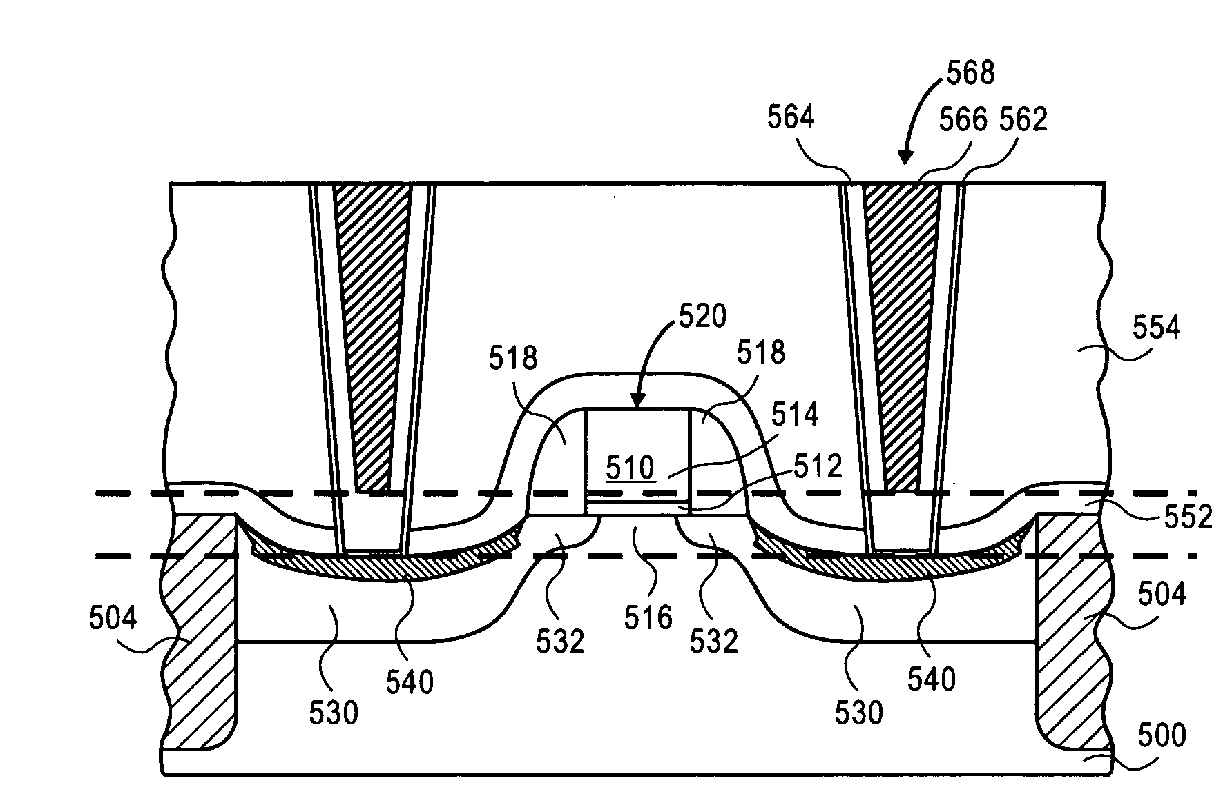
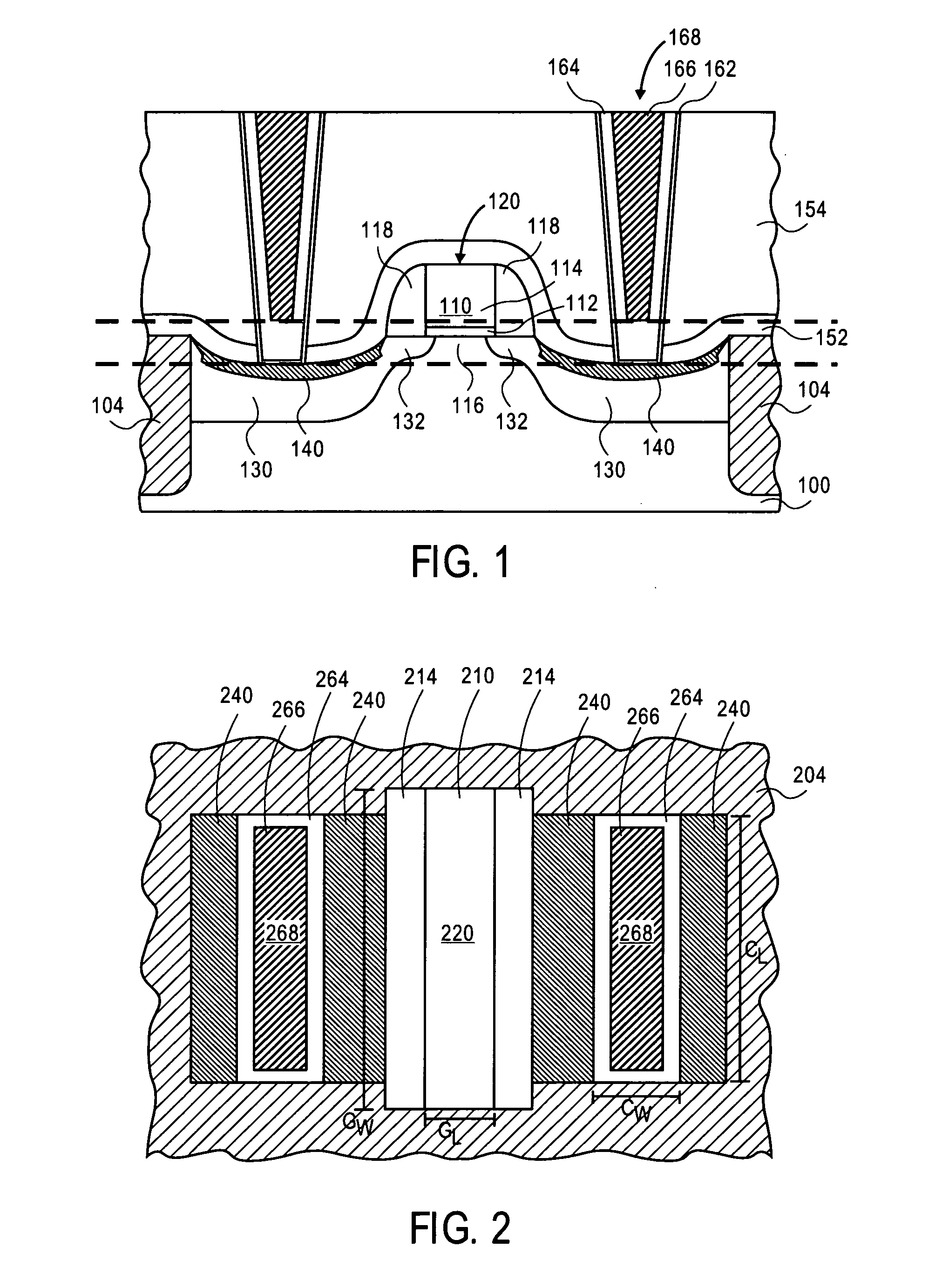
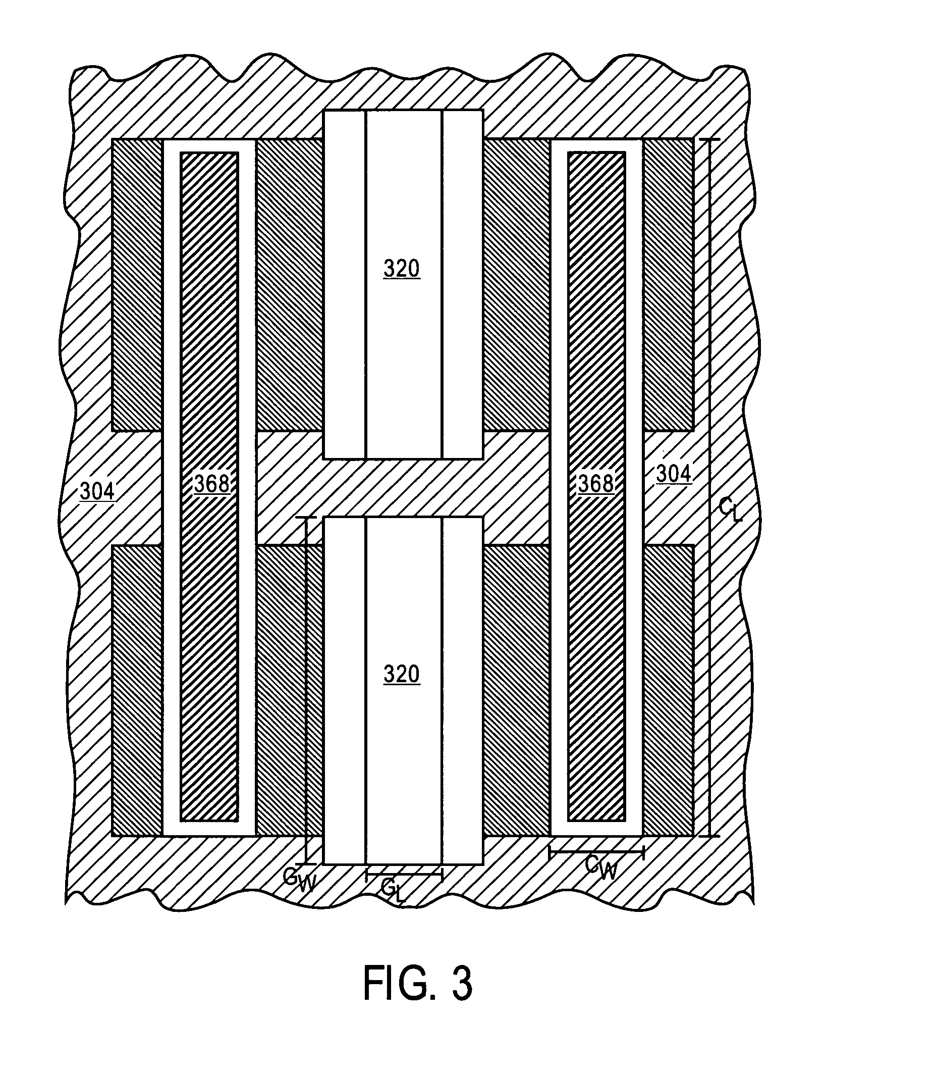
[0028]In various embodiments, a novel slot contract structure and method of fabrication is described with reference to figures. However, certain embodiments may be practiced without one or more of these specific details, or in combination with other known methods and materials. In the following description, numerous specific details are set forth, such as specific materials, dimensions and processes, etc., in order to provide a thorough understanding of the present invention. In other instances, well-known semiconductor processes and manufacturing techniques have not been described in particular detail in order to not unnecessarily obscure the present invention. Reference throughout this specification to “an embodiment” means that a particular feature, structure, material, or characteristic described in connection with the embodiment is included in at least one embodiment of the invention. Thus, the appearances of the phrase “in an embodiment” in various places throughout this speci...


PUM


Abstract

A method for forming a slot contact structure for transistor performance enhancement. A contact opening is formed to expose a contact region, and a slot contact is disposed within the contact opening in order to induce a stress on an adjacent channel region. In an embodiment, a stress inducing barrier plug is disposed within a portion of the contact opening and the remainder of the contact opening is filled with a lower resistivity contact metal. By selecting the proper materials and deposition parameters, the slot contact can be tuned to induce a tensile or compressive stress on the adjacent channel region, thus being applicable for both p-type and n-type devices.

Description

BACKGROUND OF THE INVENTION[0001]1. Field of the Invention[0002]The present invention relates to the field of semiconductor processing, and more specifically to novel contact structures and their method of fabrication.[0003]2. Discussion of Related Art[0004]Well-recognized improvements in performance, functionality and economy of manufacture have led to integrated circuit designs at extreme levels of device density and reduced size of electronic structures and conductive interconnections between them. As integrated circuits become smaller, the integrated circuit speed becomes dependent not only on the transistor but also on the interconnecting pattern.[0005]Historically, continuous performance enhancement of integrated circuit design has been dictated by the advancement of optical photolithography tools and photoresist materials. However, as CMOS device size progresses further into the nano-sized regime, the associated cost of these new tools and materials can be prohibitive. And in...

Claims


Application Information

Patent Timeline
Patent Type & Authority Applications(United States)
IPC IPC(8): H01L29/768H01L21/336
CPCH01L21/28518H01L21/2855H01L2924/0002H01L21/76843H01L21/76895H01L21/823807H01L21/823814H01L21/823871H01L23/485H01L23/53238H01L29/165H01L29/665H01L29/66628H01L29/66636H01L29/7833H01L29/7843H01L29/7845H01L29/7848H01L2924/00
Inventor FISCHER, KEVIN J.CHIKARMANE, VINAY B.PETERSON, BRENNAN L.
Owner INTEL CORP
Why Eureka
Try Eureka