Avoiding errors in a flash memory by using substitution transformations

a technology of substitution transformation and flash memory, applied in the field of flash memory, can solve the problems of reducing the effect of various undesirable phenomena, reducing the reliability reducing the error rate of flash memory devices, so as to reduce the effect, reduce the error rate, and reduce the reliability

Inactive Publication Date: 2008-07-03
RAMOT AT TEL AVIV UNIV LTD
View PDF7 Cites 109 Cited by
  • Summary
  • Abstract
  • Description
  • Claims
  • Application Information

AI Technical Summary

Benefits of technology

[0024]As noted above, if the user data are statistically distributed in such a way that higher voltage levels are frequently programmed, then the flash memory device will suffer from higher error rates and become less reliable. By manipulating the user data, we can control the distribution of states over the programmed cells. This can be used for reducing the effect of various undesirable phenomena in the flash device such as PD and such as increased charge leakage due to faster cell insulation layer weakening. For example, by limiting the fraction of cells that are programmed to low voltage levels we can reduce the number of cells that suffer from PD and as a result reduce the overall cell error rate and increase the reliability of the flash memory device. Alternatively, by limiting the fraction of cells that are programmed to high voltage levels, we can increase the effective number of P / E cycles that the flash memory device can endure because we slow down the weakening of the cells' insulation layers. Moreover, when high voltage levels are less frequently programmed, the overall stress applied to the flash cells is smaller and has shorter duration and this reduces the effect of various undesirable phenomena in the flash memory such as PD. Hence by controlling the distribution of programmed states in the flash cells, such that very low and very high states are less frequently programmed, we can increase the reliability, P / E cycle endurance and data retention time of the flash device.

Problems solved by technology

As noted above, if the user data are statistically distributed in such a way that higher voltage levels are frequently programmed, then the flash memory device will suffer from higher error rates and become less reliable.
Moreover, when high voltage levels are less frequently programmed, the overall stress applied to the flash cells is smaller and has shorter duration and this reduces the effect of various undesirable phenomena in the flash memory such as PD.

Method used


Image

  • Avoiding errors in a flash memory by using substitution transformations
  • Avoiding errors in a flash memory by using substitution transformations
  • Avoiding errors in a flash memory by using substitution transformations

Examples


Embodiment Construction

[0062]The principles and operation of a flash memory according to the present invention may be better understood with reference to the drawings and the accompanying description.

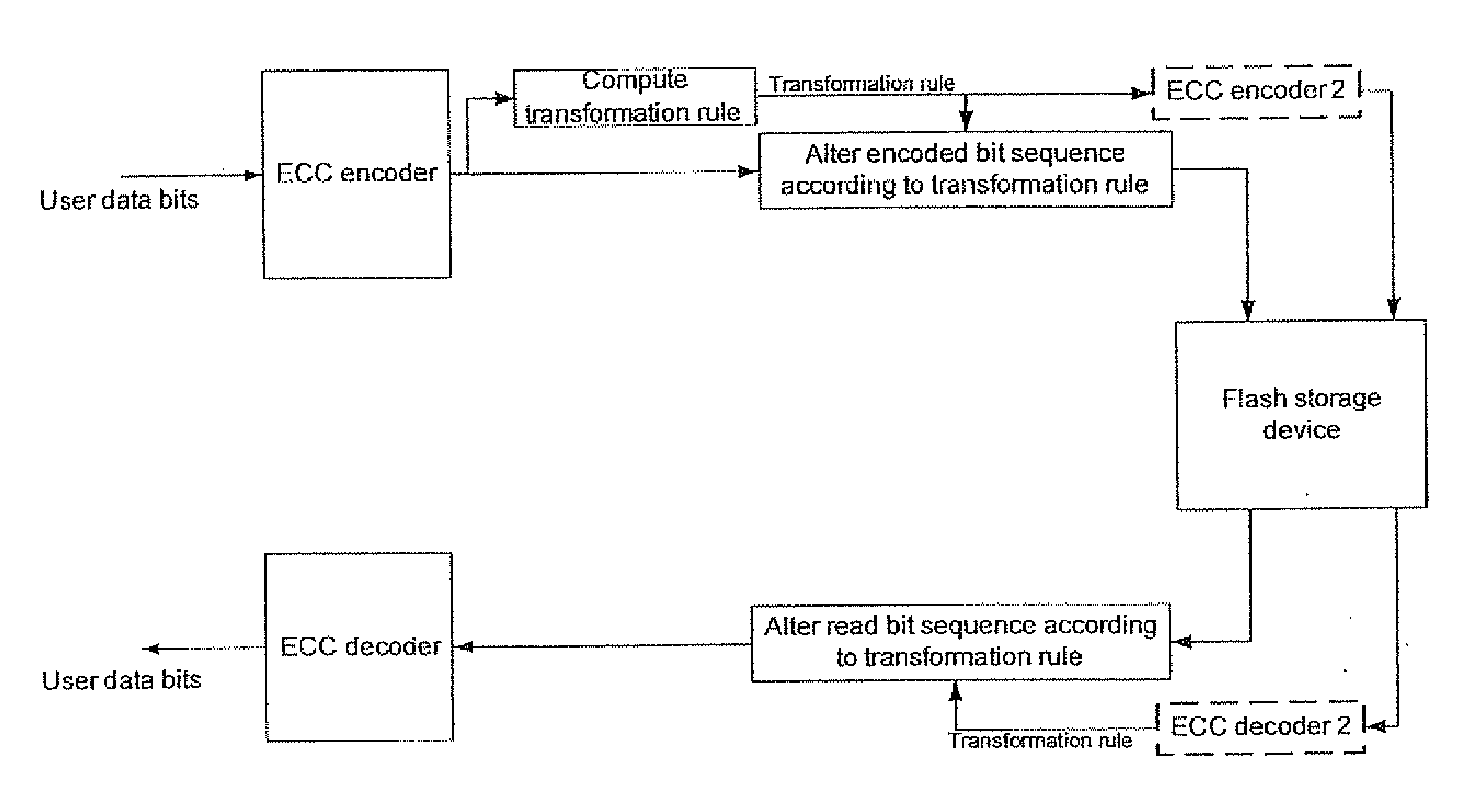
[0063]The present invention reduces the effect of error sources such as PD that depend on the user data stored in a multi bit per cell flash memory device by manipulating the user data and controlling the actual sequence of states that is programmed into the flash memory.

[0064]According to the present invention, a desired distribution states, that is optimal in the sense of minimizing the expected number of cell errors, is induced over the flash memory cells. For example, in some embodiments of the present invention the expected number of cell errors is minimized by minimizing the number of cells that are programmed to the erase state and / or to high states. This is done in the following way: The distribution of the states that should be programmed into the flash memory is examined as a function of the bit seq...


PUM


Abstract

To store an input string of M N-tuples of bits, a substitution transformation is selected in accordance with the input string and is applied to the input string to provide a transformed string of M N-tuples of bits. M or more memory cells are programmed to represent the transformed string and preferably also to represent a key of the transformation. Alternatively, the memory selectively programs each of M or more cells to a respective one of 2N states. A mapping that maps the binary numbers in [0,2N−1] into respective states is selected in accordance with the input string and is used to program M cells to represent the input string. Preferably, a key of the mapping is stored in the memory in association with the M cells.

Description

[0001]This patent application claims the benefit of U.S. Provisional Patent Application No. 60 / 882,933, filed Dec. 31, 2006FIELD AND BACKGROUND OF THE INVENTION[0002]The present invention relates to flash memories and, more particularly, to methods of transforming data for more reliable storage in a flash memory.[0003]Flash memory devices have been known for many years. Typically, each cell within a flash memory stores one bit of information. Traditionally, the way to store a bit has been by supporting two states of the cell—one state represents a logical “0” and the other state represents a logical “1”. In a flash memory cell the two states are implemented by having a floating gate above the cell's channel (the area connecting the source and drain elements of the cell's transistor), and having two valid states for the amount of charge stored within this floating gate. Typically, one state is with zero charge in the floating gate and is the initial unwritten state of the cell after ...

Claims


Application Information

Patent Timeline
Patent Type & Authority Applications(United States)
IPC IPC(8): G11C16/04
CPCG06F11/1072G11C29/00G11C11/5628G11C7/1006G06F11/10G06F12/16G11C7/10G11C11/56
Inventor SHARON, ERANLITSYN, SIMONALROD, IDAN
Owner RAMOT AT TEL AVIV UNIV LTD
Why Eureka
Try Eureka