Caching device for NAND flash translation layer

Active Publication Date: 2008-07-03
GENESYS LOGIC INC
View PDF3 Cites 48 Cited by
  • Summary
  • Abstract
  • Description
  • Claims
  • Application Information

AI Technical Summary

Benefits of technology

[0008]Accordingly, the present invention provides a space-efficient caching mechanism for the NAND flash trans

Problems solved by technology

Such an access characteristic of the NAND flash memory presents a difficulty in its management.
However, the block-level mapping is inefficient in mapping logical addresses to the p

Method used


Image

  • Caching device for NAND flash translation layer
  • Caching device for NAND flash translation layer
  • Caching device for NAND flash translation layer

Examples


Embodiment Construction

[0018]The following descriptions are exemplary embodiments only, and are not intended to limit the scope, applicability or configuration of the invention in any way. Rather, the following description provides a convenient illustration for implementing exemplary embodiments of the invention. Various changes to the described embodiments may be made in the function and arrangement of the elements described without departing from the scope of the invention as set forth in the appended claims.

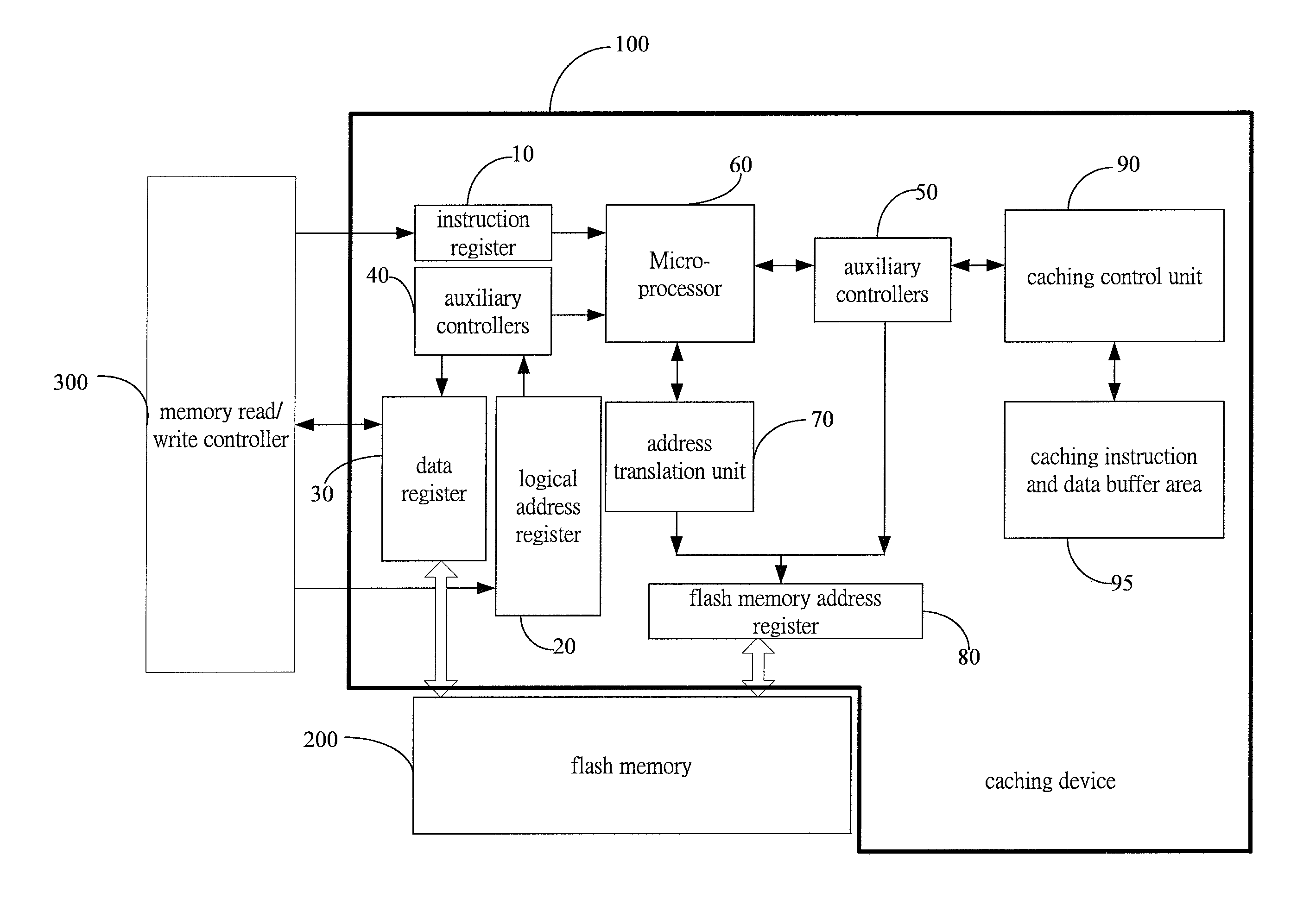
[0019]With reference to the drawings and in particular to FIG. 1, which is a schematic diagram showing a caching device, generally designated with reference numeral 100, according to the present invention, as illustrated, the caching device 100 is configured between a flash memory 200 and a memory read / write controller 300 that is one conventionally found in a flash memory card reader or in a card interface of a personal computer. The caching device 100 contains an instruction register 10, a logical...


PUM


Abstract

A caching device is positioned between a memory read/write controller and a flash memory, which contains an instruction register, a logical address register, a data register, a pair of auxiliary controllers, a microprocessor, an address translation unit, a flash memory address register, a caching control unit, and a caching instruction and data buffer area. Among them, the microprocessor is the core of the caching device responsible not only for the reading and writing the flash memory but also for the caching operation for logical and physical address translation. The caching control unit is a programmable device containing the instruction and data for caching the logical and physical address mapping. The caching instruction and data buffer area temporarily stores the caching instruction and data used by the caching control unit.

Description

BACKGROUND OF THE INVENTION[0001]1. Field of the Invention[0002]The present invention generally relates to the management of NAND flash memory, and more particularly to a caching device for NAND flash translation layer of the NAND flash memory.[0003]2. The Prior Arts[0004]Flash memories are commonly found in computers and consumer electronic products. For example, USB disks and MP3 players are the two most common applications of the flash memories. Among various types of flash memories, the NAND flash memories are commonly found in embedded systems. A NAND flash memory is organized into fixed-size pages (for example 512 bytes per page) and a number of pages constitute a block (for example 32 pages per block). A characteristic of the NAND flash memory is that two pages of the same block cannot be written simultaneously unless that block is erased first. Such an access characteristic of the NAND flash memory presents a difficulty in its management.[0005]To make a NAND flash memory to ...

Claims


Application Information

Patent Timeline
IPC IPC(8): G06F12/02
CPCG06F12/0246G06F2212/7203G06F2212/7201
Inventor WU, CHIN-HSIENKUO, TEI-WEIHSIEH, HSIANG-CHI
Owner GENESYS LOGIC INC
Why Eureka
Try Eureka