Uniform critical dimension size pore for pcram application

a critical dimension and pore technology, applied in the field of computer memory, can solve the problem that the change material does not utilize chalcogen

Inactive Publication Date: 2008-07-10
IBM CORP +1
View PDF24 Cites 109 Cited by
  • Summary
  • Abstract
  • Description
  • Claims
  • Application Information

AI Technical Summary

Problems solved by technology

However, some phase change materials do not utilize chalcogen, such as GeSb.

Method used


Image

  • Uniform critical dimension size pore for pcram application
  • Uniform critical dimension size pore for pcram application
  • Uniform critical dimension size pore for pcram application

Examples


Embodiment Construction

[0017]The present invention is described herein with reference to embodiments of the invention. Throughout the description of the invention reference is made to FIGS. 1-8. When referring to the figures, like structures and elements shown throughout are indicated with like reference numerals.

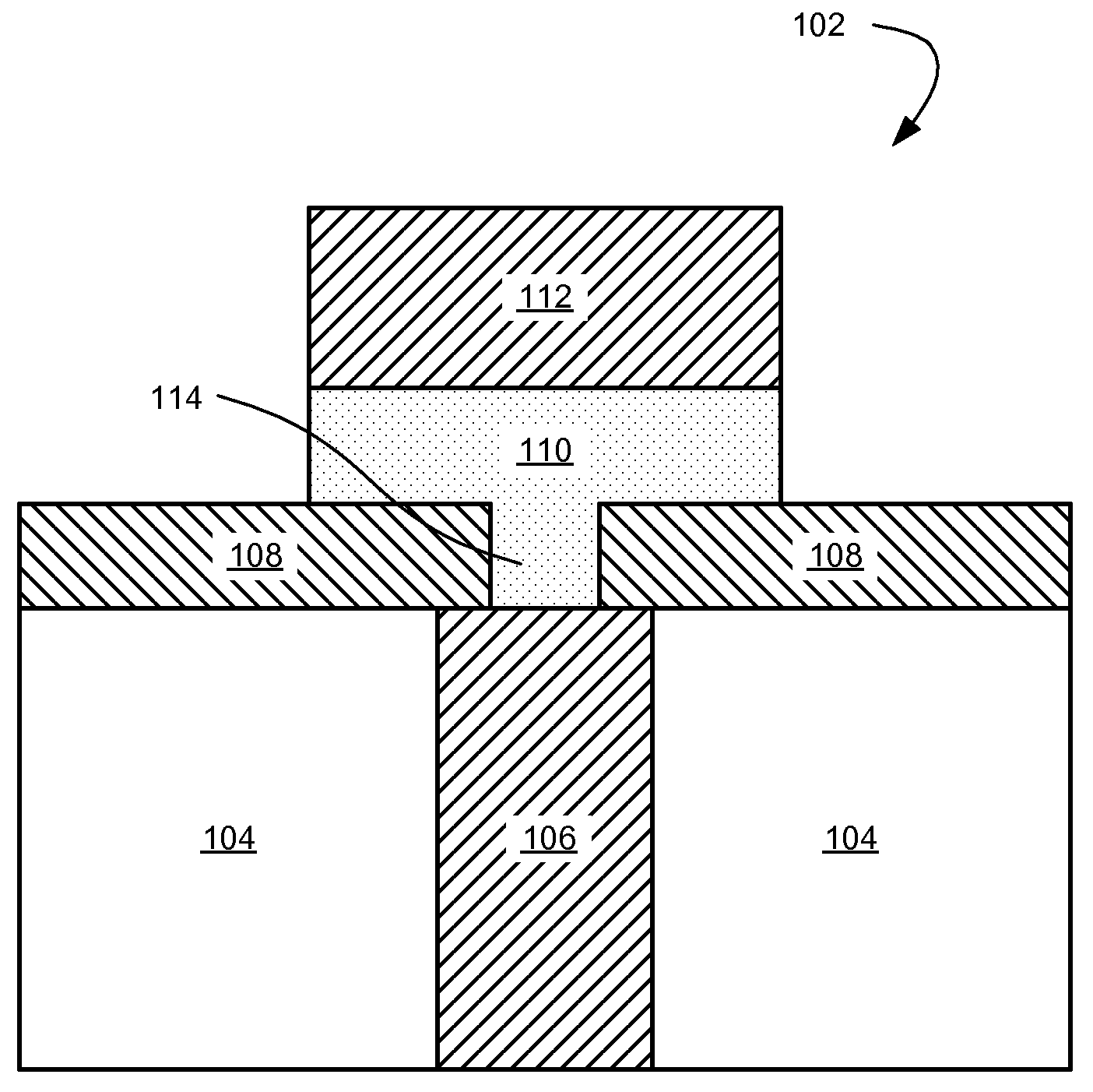
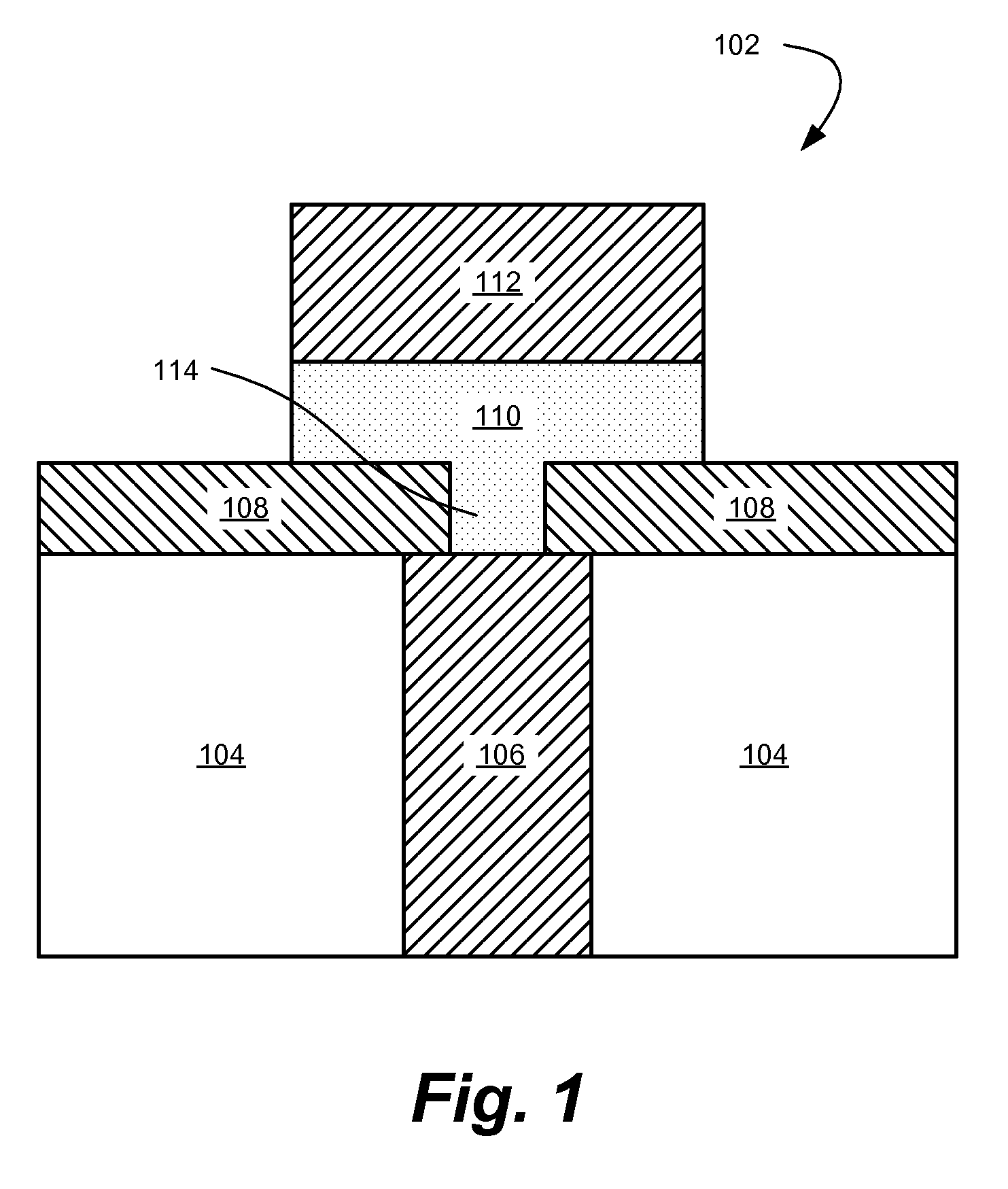
[0018]FIG. 1 illustrates the cross sectional view of an exemplary memory cell 102 contemplated by the present invention. The exemplary memory cell 102 is comprised of an insulating layer 104, a bottom electrode 106, an intermediate insulating layer 108, a pore 114 within the intermediate insulating layer that contains phase change material 110, and an upper electrode 112. The memory cell 102 is typically formed on a substrate with metal-oxide-semiconductor field-effect transistors (MOSFETs) (not shown). Other switching devices known to those skilled in the art, such as junction FETs and bipolar junction transistors, may be used with the present invention.

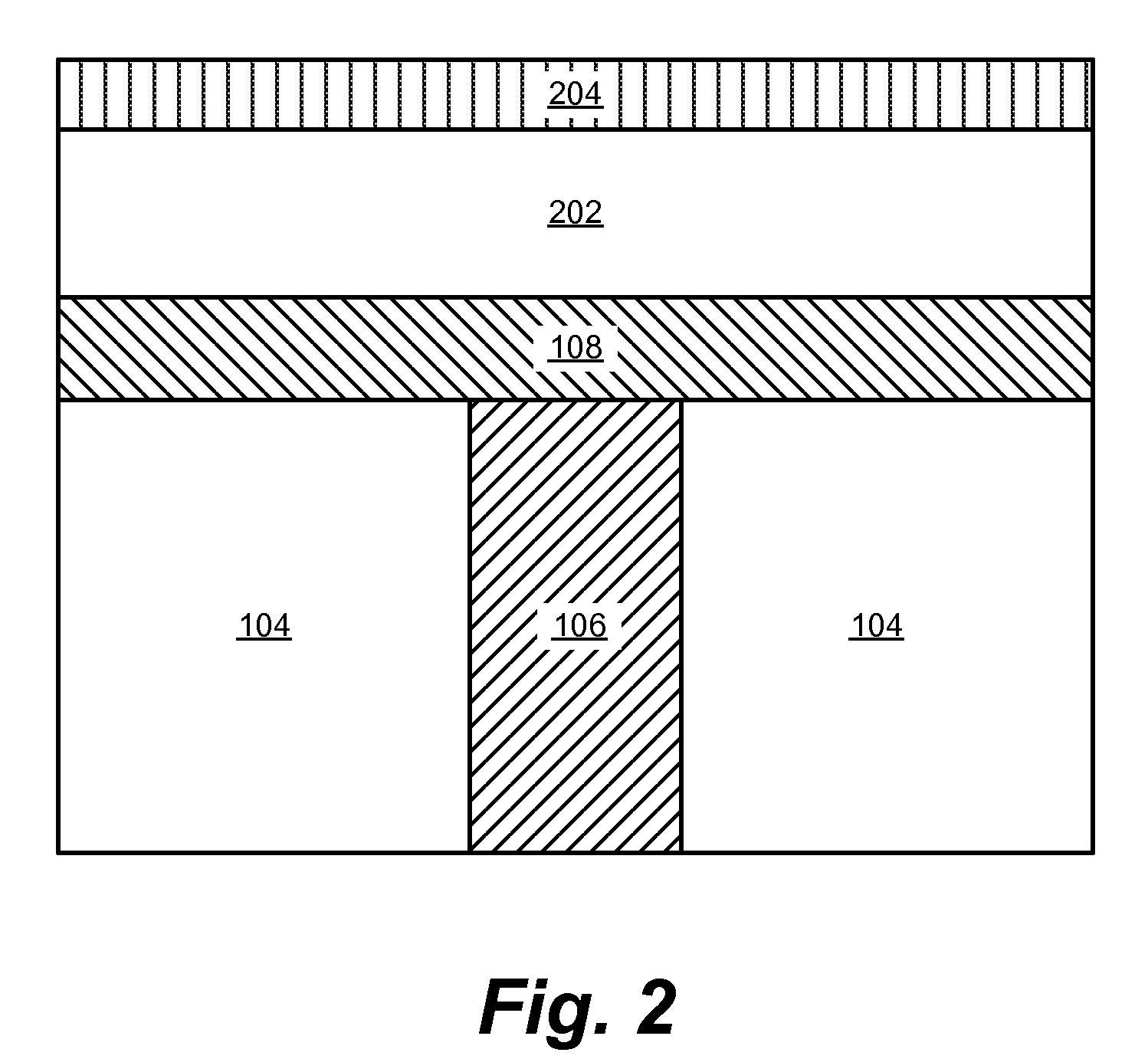
[0019]In FIG. 2 an exemplary embodiment of...


PUM

PropertyMeasurementUnit
thicknessaaaaaaaaaa
diameteraaaaaaaaaa
thickaaaaaaaaaa

Abstract

A memory cell and a method of making the same, that includes insulating material deposited on a substrate, a bottom electrode formed within the insulating material, a plurality of insulating layers deposited above the bottom electrode and at least one of which acts as an intermediate insulating layer. A via is defined in the insulating layers above the intermediate insulating layer. A channel is created for etch with a sacrificial spacer. A pore is defined in the intermediate insulating layer. All insulating layers above the intermediate insulating layer are removed, and the entirety of the remaining pore is filled with phase change material. An upper electrode is formed above the phase change material.

Description

FIELD OF THE INVENTION[0001]The present invention is directed toward computer memory, and more particularly to a non-volatile phase change memory device.BACKGROUND OF THE INVENTION[0002]There are two major groups in computer memory: non-volatile memory and volatile memory. Constant input of energy in order to retain information is not necessary in non-volatile memory but is required in the volatile memory. Examples of non-volatile memory devices are Read Only Memory, Flash Electrical Erasable Read Only Memory, Ferroelectric Random Access Memory, Magnetic Random Access Memory, and Phase Change Memory. Examples of volatile memory devices include Dynamic Random Access Memory (DRAM) and Static Random Access Memory (SRAM). The present invention is directed to phase change memory. In phase change memory, information is stored in materials that can be manipulated into different phases. Each of these phases exhibit different electrical properties which can be used for storing information. T...

Claims


Application Information

Patent Timeline
Patent Type & Authority Applications(United States)
IPC IPC(8): H01L47/00H01L21/28
CPCH01L45/06H01L45/1233H01L45/1683H01L45/148H01L45/144H10N70/231H10N70/826H10N70/884H10N70/8828H10N70/066
Inventor BREITWISCH, MATTHEW J.CHEEK, ROGER W.LAM, CHUNG H.LUNG, HSIANG-LANJOSEPH, EIRC A.SCHROTT, ALEJANDRO G.
Owner IBM CORP
Why Eureka
Try Eureka