Method and Apparatus for Providing Thermal Management on High-Power Integrated Circuit Devices

a technology of integrated circuit devices and thermal management, which is applied in the direction of electrical equipment, semiconductor devices, semiconductor/solid-state device details, etc., can solve the problems of increasing the operating temperature of the integrated circuit device, increasing the difficulty of thermal management, and no longer being effective, and achieves high thermal conductivity

Active Publication Date: 2008-07-10
BAE SYST INFORMATION & ELECTRONICS SYST INTERGRATION INC
View PDF11 Cites 15 Cited by
  • Summary
  • Abstract
  • Description
  • Claims
  • Application Information

AI Technical Summary

Problems solved by technology

Integrated circuit devices generally dissipate more heat as their performances increase, which can increase the operating temperature of the integrated circuit devices.
Such a problem is becoming more acute as the size of silicon chips become larger yet the sizes of the electronic components within the silicon chips approach nanometer scale.
The prior art methods of integrated circuit cooling were effective when chip powers were uniformly distributed with a total of less than one watt, but are no longer effective as chip powers exceed five watts and are generally focused in very small areas at a circuit level.
To effectively cool small regions of an integrated circuit device at a circuit level under the above-mentioned power conditions using traditional methods of integrated circuit cooling would require such an over-design in the rest of the silicon chip that it becomes too impractical to implement.

Method used


Image

  • Method and Apparatus for Providing Thermal Management on High-Power Integrated Circuit Devices
  • Method and Apparatus for Providing Thermal Management on High-Power Integrated Circuit Devices
  • Method and Apparatus for Providing Thermal Management on High-Power Integrated Circuit Devices

Examples


Embodiment Construction

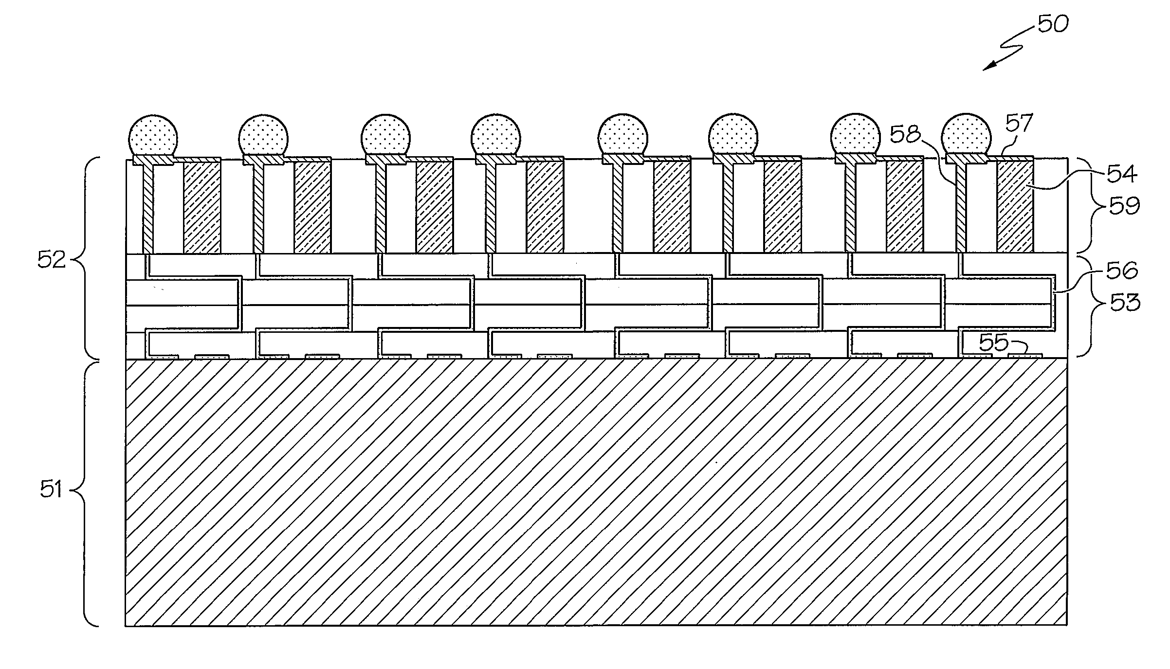
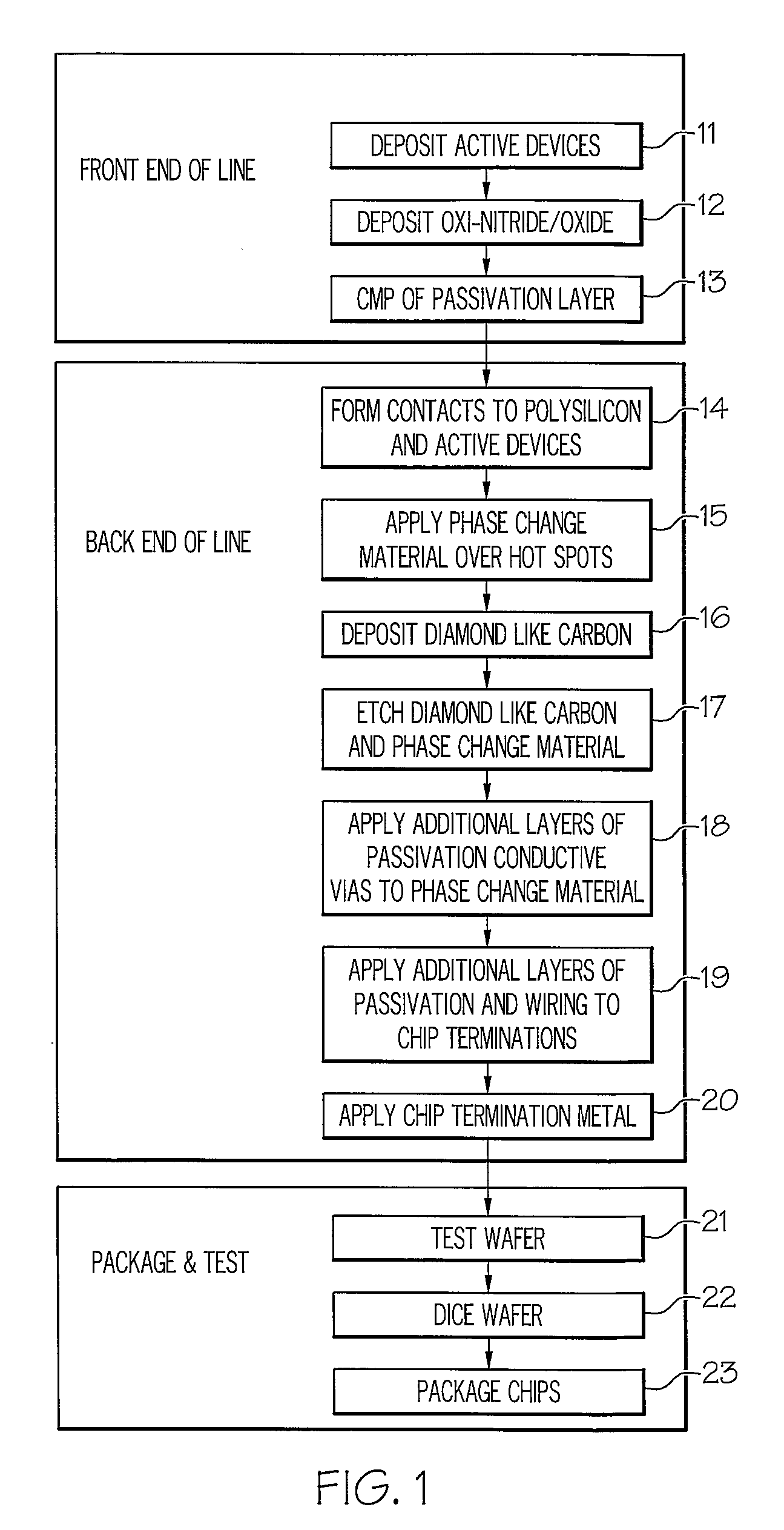
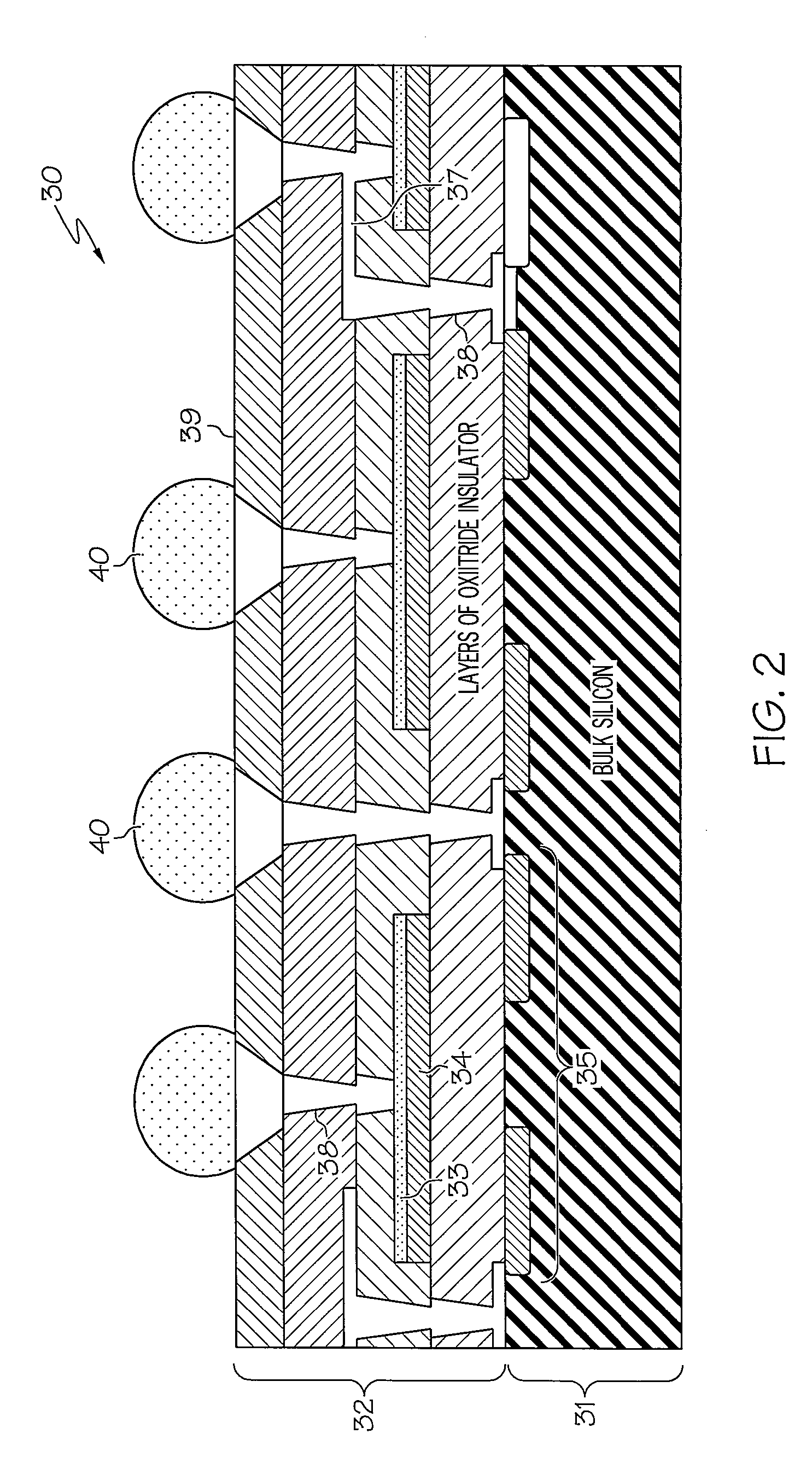
[0013]During the normal operation of an integrated circuit device, there are localized, thermal transients occurring across the active surface of the silicon chip. These hot spots are caused by high-power function circuits found at specific locations on the chip. Such situation becomes more acute as the chip operates faster with smaller features. It is often found that high-power function circuits are dissipating large amount of power by cycling on and off at a very high rate of speed. For some high-power function circuits, a series of gates switch on at the beginning of a duty cycle, drawing a sudden current spike and then not drawing any significant power for the remainder of the duty cycle. A typical duty cycle for many high-power function circuits is approximately 30 ns, and a 4 ns surge can occur within the first 7 ns of the cycle. It is during such sudden current surge that most of the power for the high-power function circuit is dissipated.

[0014]A thermal management scheme th...


PUM


Abstract

An apparatus for providing thermal management on high-power integrated circuit devices is disclosed. Initially, contacts to active devices are formed. Phase change materials are then applied over potential hot spots that can be formed by the active devices. A layer of high-thermally conductive materials is deposited over the phase change materials. The layer of high-thermally conductive materials and the phase change materials are subsequently etched according to a pattern. A layer of passivation conductive vias is subsequently applied to the phase change materials to complete the formation of phase change heatsinks.

Description

BACKGROUND OF THE INVENTION[0001]1. Technical Field[0002]The present invention relates to thermal management in general, and in particular to thermal management on electronic devices. Still more particularly, the present invention relates to a method and apparatus for providing thermal management on high-power integrated circuit devices.[0003]2. Description of Related Art[0004]Integrated circuit devices generally dissipate more heat as their performances increase, which can increase the operating temperature of the integrated circuit devices. Such a problem is becoming more acute as the size of silicon chips become larger yet the sizes of the electronic components within the silicon chips approach nanometer scale.[0005]The prior art methods of integrated circuit cooling typically employ conduction and convection cooling at a device level by attaching a heatsink to one of the surfaces of an integrated circuit device, and ambient air is forced over the heatsink to carry heat away from...

Claims


Application Information

Patent Timeline
Patent Type & Authority Applications(United States)
IPC IPC(8): H01L23/34H01L21/00
CPCH01L21/4871H01L23/3677H01L2224/13H01L23/427H01L23/3732H01L24/05H01L24/06H01L2224/0554H01L2224/05573H01L2224/05684H01L2224/06519H01L2224/13006H01L2224/13023H01L2224/131H01L2224/14519H01L2924/00014H01L2224/05599H01L2224/0555H01L2224/0556H01L2924/014H01L2224/13025
Inventor STURCKEN, KEITH K.MCINTYRE, THOMAS J.
Owner BAE SYST INFORMATION & ELECTRONICS SYST INTERGRATION INC
Why Eureka
Try Eureka