Probe for high frequency signal transmission and probe card using the same

a high-frequency signal and probe card technology, applied in the field of probe cards, can solve the problems of dielectric loss during high-frequency signal transmission, and the inability of cantilever-type probe cards to allow a large number of probes for probing electronic devices with high-frequency signaling

Active Publication Date: 2008-07-10
MICROELECTRONICS TECH INC
View PDF13 Cites 30 Cited by
  • Summary
  • Abstract
  • Description
  • Claims
  • Application Information

AI Technical Summary

Benefits of technology

[0008]The present invention has been accomplished under the circumstances in view. It is therefore one objective of the present invention to provide a probe for use in a probe card for high frequency signal transmission, which can maintain the characteristic impedance of the high frequency test signal.

Problems solved by technology

Therefore, the parasitic capacitor induced by the surrounding dielectric environment around each coaxial probe 20 may cause dielectric loss during high-frequency signal transmission.
Therefore, the aforesaid prior art cantilever-type probe card does not allow for a big number of probes for probing electronic devices with high frequency signaling.

Method used


Image

  • Probe for high frequency signal transmission and probe card using the same
  • Probe for high frequency signal transmission and probe card using the same
  • Probe for high frequency signal transmission and probe card using the same

Examples


first embodiment

[0035]Referring to FIGS. 2-5, a cantilever-type probe card 2 for testing semiconductor wafers or the like in accordance with the present invention comprises a circuit board 30, a probe holder 40, a plurality of signal probes 50, and a plurality of grounding probes 60.

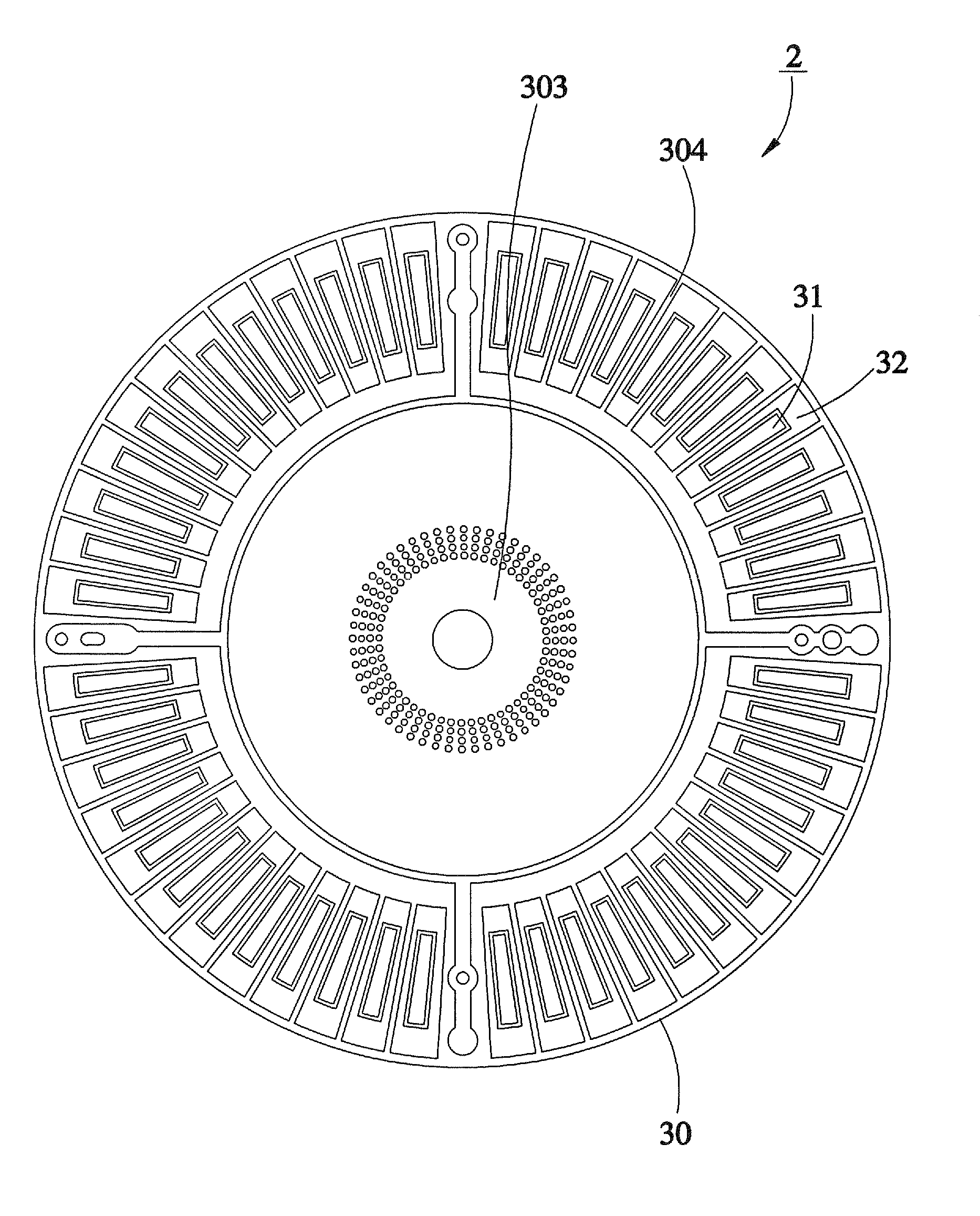
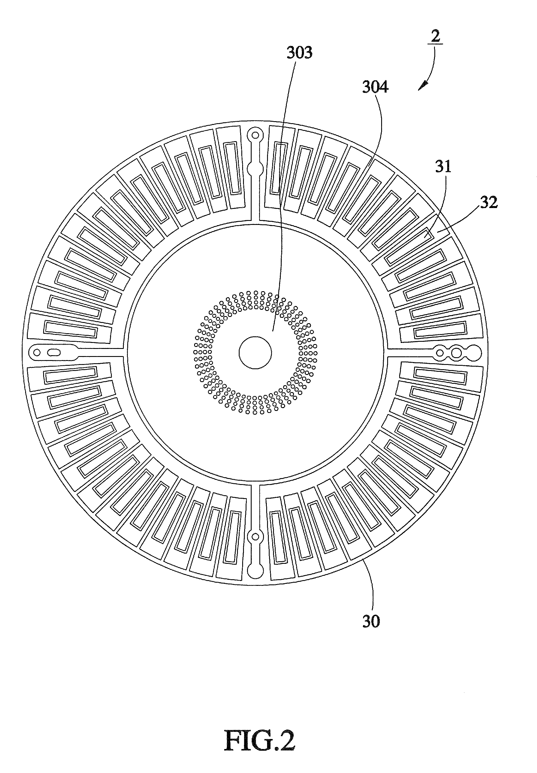
[0036]As shown in FIGS. 2 and 3, the circuit board 30 defines a top surface 301 and a bottom surface 302 opposite to the top surface 301, and is divided into an inner probing zone 303 and an outer testing zone 304 around the inner probing zone 303. The outer testing zone 304 at the top surface 301 is to be electrically connected to a test machine (not shown), which is controllable to output an electrical test signal to the probe card 2 for providing a high frequency test signal to the inner probing zone 303. The circuit board 30 has arranged thereon electronic circuits including multiple signal circuits 31 and grounding circuits 32, which extend from the top surface 301 to the bottom surface 302 and are electrically con...

second embodiment

[0042]FIG. 9 is a cross sectional view of a signal probe 53 in accordance with the present invention. According to this embodiment, the signal probe 53 comprises a metal pin 51 and two lead wires 52 abutted at two opposite sides of the metal pin 51. This embodiment prevents the possibility of signal interference at one side of the metal pin without lead wire, thereby having excellent transmission quality during high frequency signaling.

third embodiment

[0043]FIG. 10 is a cross sectional view of a signal probe 55 in accordance with the present invention. According to this embodiment, the signal probe 55 comprises a metal pin 51, an insulated layer 54 surrounding the metal pin 51 coaxially, and a metal line 520 arranged on the periphery of the insulated layer 54. This embodiment protects the metal pin 51 against oxidation or contamination, thereby prolonging the service life of the metal pin 51.

[0044]FIG. 11 illustrates a cantilever-type probe card 3 in accordance with a fourth embodiment of the present invention. This embodiment is substantially similar to the aforesaid first embodiment with the exception that the probe holder 40 according to this fourth embodiment has a grounding surface 41 made of a conducting metal material, and the metal lines 520 of the signal probes 50 and the grounding pins 60 are electrically connected to the grounding surface 41. The grounding surface 411 provides the cantilever-type probe card 3 with an e...


PUM


Abstract

A probe for high frequency signal transmission includes a metal pin, and a metal line spacedly arranged on and electrically insulated from the metal pin and electrically connected to grounding potential so as to maintain the characteristic impedance of the probe upon transmitting high frequency signal. The maximum diameter of the probe is substantially equal to or smaller than two times of the diameter of the metal pin. Under this circumstance, a big amount of probes can be installed in a probe card for probing a big amount of electronic devices, so that a wafer-level electronic test can be achieved efficiently and rapidly.

Description

BACKGROUND OF THE INVENTION[0001]1. Field of the Invention[0002]The present invention relates generally to probe cards and more particularly, to a probe adapted to be used in a probe card for high frequency signal transmission.[0003]2. Description of the Related Art[0004]FIG. 1 shows a cantilever-type probe card 1 according to a design of prior art. According to this design, the cantilever-type probe card 1 comprises a circuit board 10, a plurality of coaxial transmission lines 11 arranged around the outer area of the circuit board 10, a probe holder 12 arranged on the inner area of the circuit board 10, and a plurality of coaxial probes 20. The probe holder 12 comprises an insulated base 121 made of a shock-absorbable electrically insulated material, a grounding body 122 made of a metal material and disposed on the insulated base 121 and electrically connected to grounding potential of the cantilever-type probe card 1, and a plurality of locating members 123 fixedly provided on the...

Claims


Application Information

Patent Timeline
Patent Type & Authority Applications(United States)
IPC IPC(8): G01R1/067
CPCG01R1/06772H01L22/00
Inventor KU, WEI-CHENGHO, CHIH-HAOCHANG, CHIA-TAILIN, HO-HUILIN, CHIEN-HO
Owner MICROELECTRONICS TECH INC
Why Eureka
Try Eureka