Liquid crystal device and electronic apparatus

a technology of electronic equipment and liquid crystal, which is applied in the direction of static indicating equipment, instruments, non-linear optics, etc., can solve the problems of strict regulation, occurrence of assembly deviation, complex electrical structure of electrodes and wiring structures in the pair of substrates, etc., and achieves the effect of increasing the thickness of the electronic apparatus and thin overall thickness

Inactive Publication Date: 2008-07-10
JAPAN DISPLAY WEST
View PDF5 Cites 16 Cited by
  • Summary
  • Abstract
  • Description
  • Claims
  • Application Information

AI Technical Summary

Benefits of technology

[0034]The third liquid crystal device differs from the second liquid crystal device in that, in the second liquid crystal device, a pigmented film of the same color but lighter than the color of a pigmented film used in the display pixels adjacent to the viewing angle control pixel is provided in each of the viewing angle control pixels, whereas, in the third liquid crystal device, a pigmented film having the same characteristic used as a pigmented film in the display pixels adjacent to the viewing angle control pixel but partly having a non-pigmented region is provided in each of the viewing angle control pixels. That is, in the second liquid crystal device, a pigmented film having a uniform color depth is provided in each of the viewing angle control pixels, whereas, in the third liquid crystal device, a region at which a pigmented film is removed is provided in each of the viewing angle control pixels. According to this configuration, when vie

Problems solved by technology

However, in the above Non-Patent Document 1, it is necessary to provide electrodes respectively for a pair of substrates opposite each other in order to form a vertical electric field within the viewing angle control pixels and, therefore, there is a problem that an electrode structure and a wiring structure are complex in the pair of substrates.
In addition, there is also a problem that an occurrence of assembly deviation when the pair of substrates are adhered should be strictly regulated.
On the other hand, when an on voltage is applied to the viewing angle control pixels while wide viewing angle display is being performed using the display pixels on t

Method used


Image

  • Liquid crystal device and electronic apparatus
  • Liquid crystal device and electronic apparatus
  • Liquid crystal device and electronic apparatus

Examples


first embodiment

of Liquid Crystal Device

[0056]Hereinafter, an embodiment of the invention will be described by taking a case where the invention is applied to an transmissive active matrix mode liquid crystal device, which is able to perform color display, as an example of a liquid crystal device. In addition, in the present embodiment, the aspects of the invention are applied to a liquid crystal device that uses a channel-etch-type single gate polysilicon TFT elements as switching elements. In addition, in the liquid crystal device of the present embodiment, an FFS (Fringe Field Switching) mode, which is one of lateral electric field driving mode, is employed. Needless to say, the aspects of the invention are not limited to this embodiment. Furthermore, in the drawings used in the following description, dimensions of a plurality of components may be varied from an actual ratio thereof for the purpose of easier understanding of characterized portions.

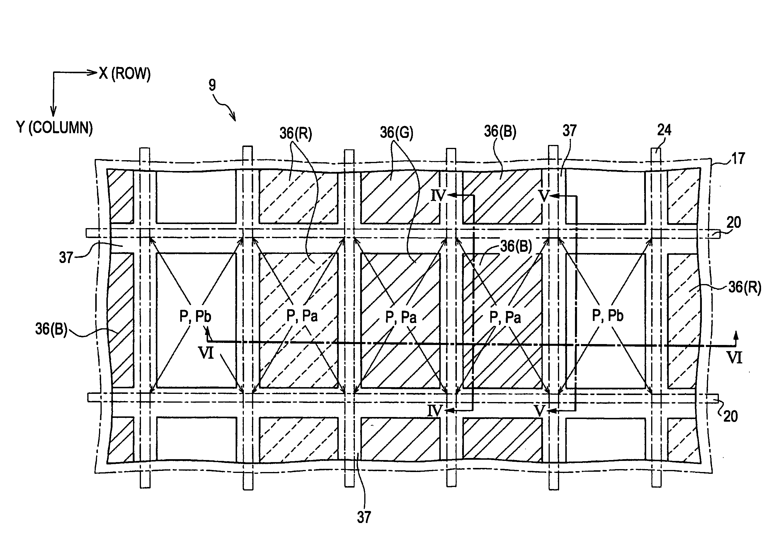
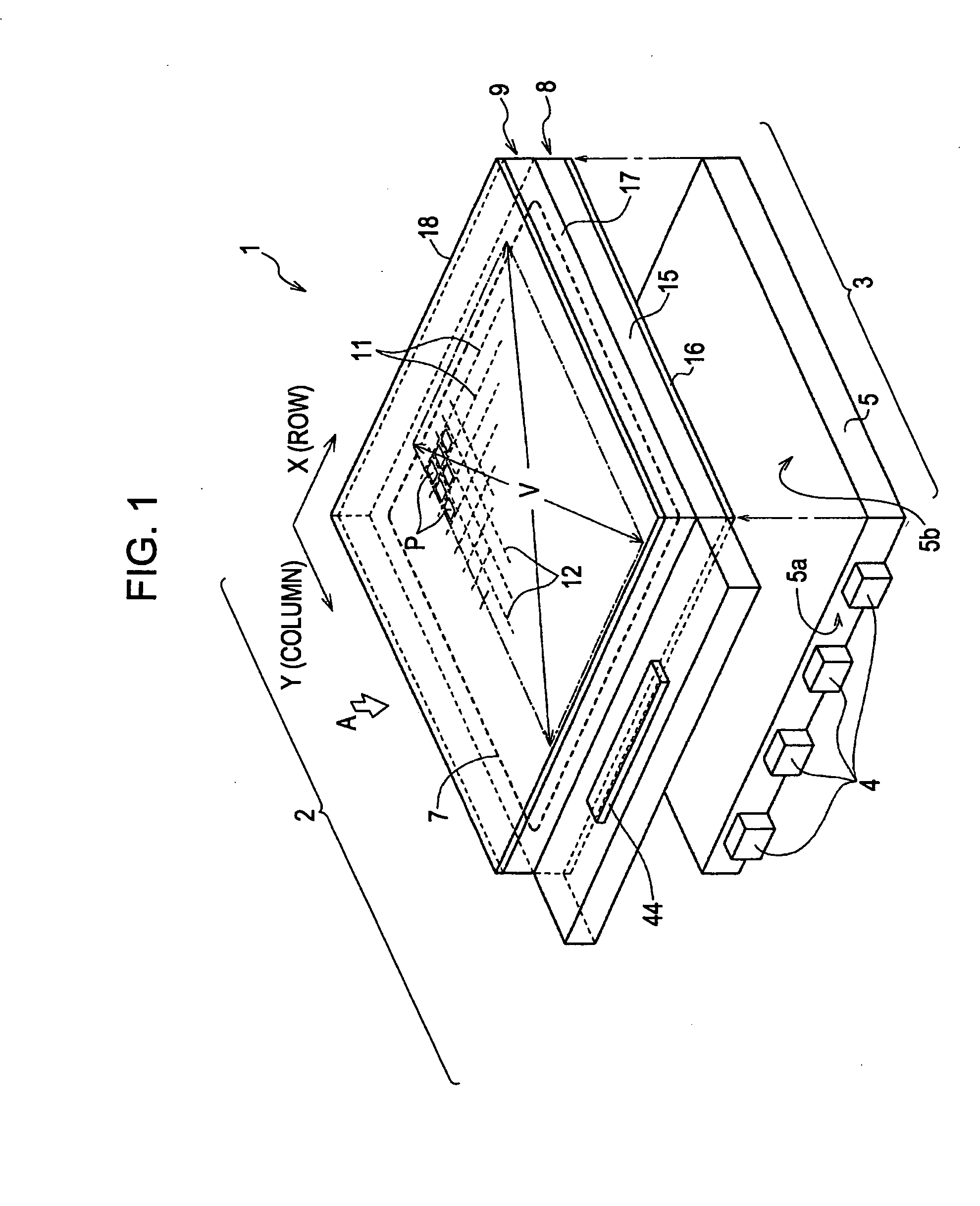
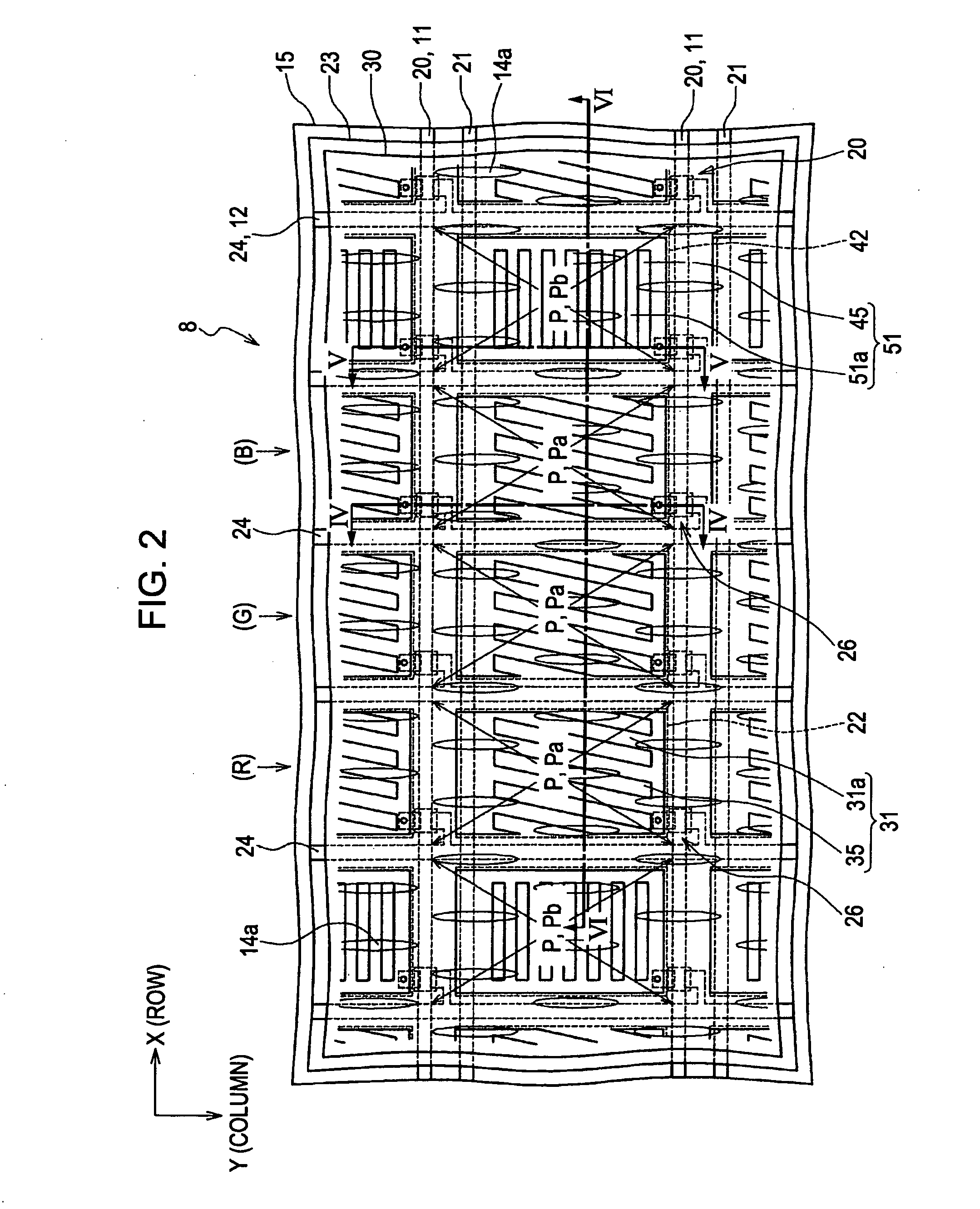
[0057]FIG. 1 is a perspective view that shows on...

second embodiment

of Liquid Crystal Device

[0097]FIG. 9 and FIG. 10 are views that show a second embodiment of the liquid crystal device according to the invention. FIG. 9 is a plan view of an element substrate corresponding to FIG. 2 of the first embodiment that is described with reference to FIG. 2 to FIG. 6. FIG. 10 is a plan view of a color filter substrate corresponding to FIG. 3 of the first embodiment. The general configuration of the liquid crystal device according to the second embodiment is the same as that of the first embodiment shown in FIG. 1.

[0098]The cross-sectional structure along the column direction Y of one sub-pixel P (particularly, display pixel Pa), taken along the line IV-IV in FIG. 9, is the same as the cross-sectional structure shown in FIG. 4 in the first embodiment. The cross-sectional structure along the column direction Y of one sub-pixel (particularly, viewing angle control pixel Pb), taken along the line V-V in FIG. 9, is the same as the cross-sectional structure shown ...

third embodiment

of Liquid Crystal Device

[0108]FIG. 11 is a view that shows a color filter substrate, which is a relevant portion of a third embodiment of the liquid crystal device according to the invention. The third embodiment shown herein is a modified embodiment that is obtained by modifying the second embodiment shown in FIG. 9 and FIG. 10. FIG. 11 is a plan view corresponding to FIG. 10 in the second embodiment and, therefore, is a plan view of the color filter substrate 9 corresponding to FIG. 3 in the first embodiment that is described with reference to FIG. 2 to FIG. 6. The element substrate used in the present embodiment is the same as the element substrate 8 shown in FIG. 9 used in the second embodiment.

[0109]FIG. 12 is a view that shows a cross-sectional structure of the viewing angle control pixel Pb along the column direction Y, taken along the line XII-XII in FIG. 11. FIG. 13 is a view that shows a cross-sectional structure of the three display pixels Pa (that is, one pixel set) alon...


PUM


Abstract

A liquid crystal device includes a first substrate, a second substrate, a liquid crystal layer, a display pixel, and a viewing angle control pixel. The liquid crystal layer is provided between the first substrate and the second substrate. The display pixels and the viewing angle control pixels are arranged in a planar region of the first substrate and second substrate to form a display area. Each of the display pixels and each of the viewing angle control pixels each drive the liquid crystal layer by electric field generated between a first electrode and a second electrode. In each of the viewing angle control pixels, a direction of a plane along which electric field is generated between the first electrode and the second electrode is substantially parallel to an initial alignment direction of liquid crystal molecules of the liquid crystal layer.

Description

[0001]The entire disclosure of Japanese Patent Application Nos. 2007-001095, filed Jan. 9, 2007 and 2007-288141, filed Nov. 6, 2007 are expressly incorporated by reference herein.BACKGROUND[0002]1. Technical Field[0003]The present invention relates to a liquid crystal device and an electronic apparatus that are provided with viewing angle control function of switching a wide viewing angle visible state and a narrow viewing angle visible state.[0004]2. Related Art[0005]Currently, a liquid crystal device is widely used in an electronic apparatus, such as a cellular phone, a personal digital assistants, or a computer display. For example, the liquid crystal device is used for displaying various pieces of information regarding an electronic apparatus as an image. In regard to this liquid crystal device, a wide viewing angle characteristic may be required or a narrow viewing angle characteristic may also be required.[0006]When a large number of people view an image that is displayed on t...

Claims


Application Information

Patent Timeline
IPC IPC(8): G02F1/1335G02F1/1333
CPCG02F1/1323G02F2001/134345G02F1/134363G02F1/134345
Inventor MATSUSHIMA, TOSHIHARU
Owner JAPAN DISPLAY WEST
Why Eureka
Try Eureka