Substrate processing apparatus, method of manufacturing semiconductor device, and reaction vessel

a processing apparatus and semiconductor technology, applied in the direction of coatings, metallic material coating processes, chemical vapor deposition coatings, etc., can solve the problems of affecting the uniformity of wafer in-plane film thickness, the necessity for a plurality of gas nozzles of different lengths, and the inability to achieve uniform thickness uniformity

Inactive Publication Date: 2008-07-24
KOKUSA ELECTRIC CO LTD
View PDF12 Cites 350 Cited by
  • Summary
  • Abstract
  • Description
  • Claims
  • Application Information

AI Technical Summary

Problems solved by technology

For example, there is a problem inherent to the apparatus shown in FIG. 18 in that, because the film formation gas is introduced from below and exhausted thereabove, the film formation gas is less likely to flow to the center of the wafers W and, accordingly, differences in film thickness between the center and outer circumferential portions of the wafers are generated and the wafer in-plane film thickness uniformity is affected.
There is a further problem inherent thereto in that, comparing the wafers W of positions in the lower part and the upper part of the wafer processing space 10, film formation differences between wafers located in the upper part and those in the lower part are generated due to consumption of the film formation gas occurring at the lower part and, accordingly, the wafers of the lower part are formed thicker and the wafer in-plane film thickness uniformity is affected.
In addition, in the apparatus shown in FIG. 19, even though the in-plane and interwafer film thickness uniformity are by and large satisfactory, the necessity for a plurality of gas nozzles of differing length translates to poor maintenance characteristics.
There is an additional problem in that, if the film formation conditions are altered, in most instances the changes in the film formation conditions cannot be accommodated without altering length and the number of the gas nozzles 16, while not altering the type of gas nozzles 16 restricts the conditions at which a film is able to be formed.
There is a problem inherent to the apparatus shown in FIG. 20 in that, because the gas nozzle 26 is provided in the wafer processing space

Method used


Image

  • Substrate processing apparatus, method of manufacturing semiconductor device, and reaction vessel
  • Substrate processing apparatus, method of manufacturing semiconductor device, and reaction vessel
  • Substrate processing apparatus, method of manufacturing semiconductor device, and reaction vessel

Examples


first embodiment

Modifications

[0109]The following range of modifications can be made to the first embodiment of the present invention described above. >

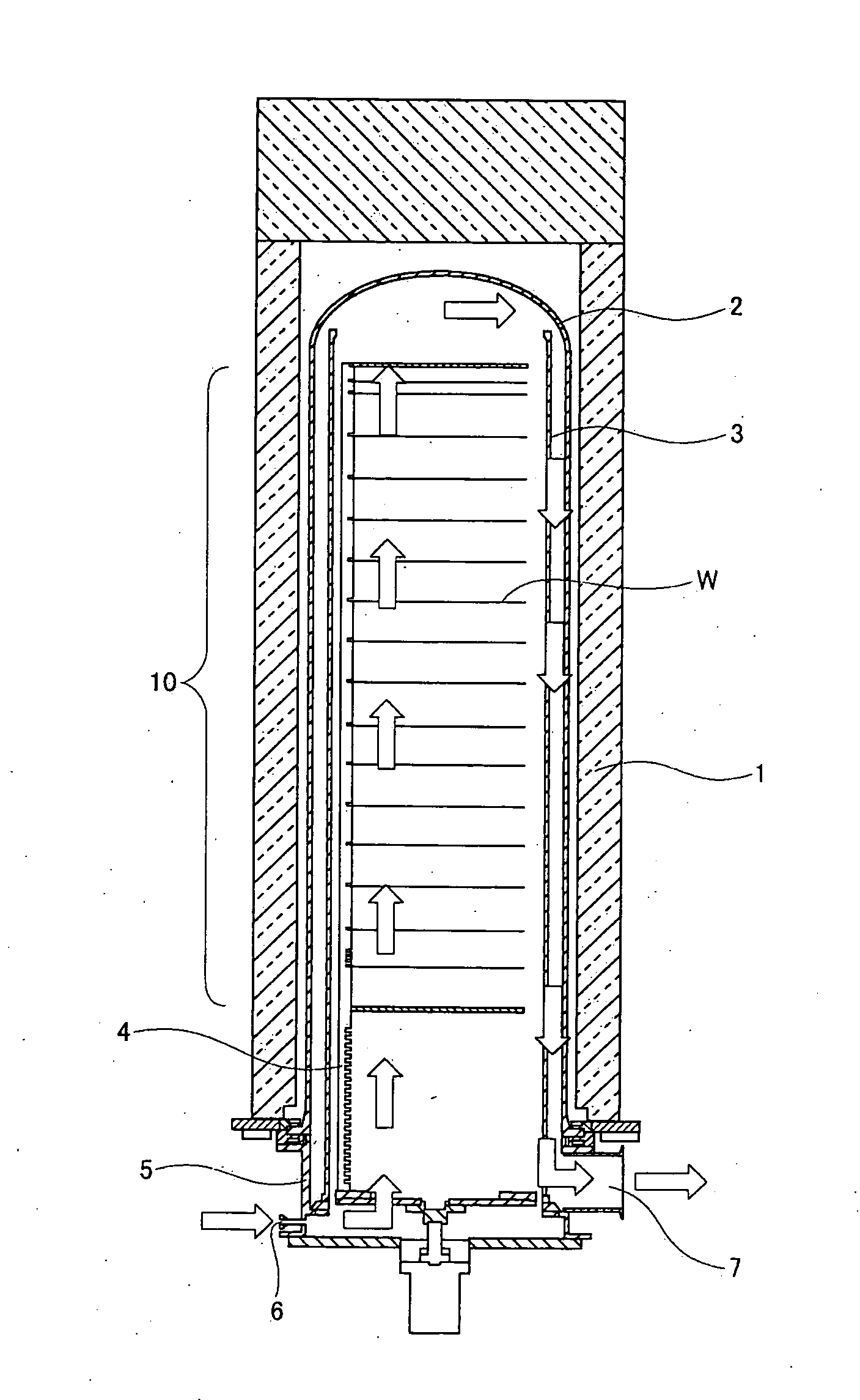
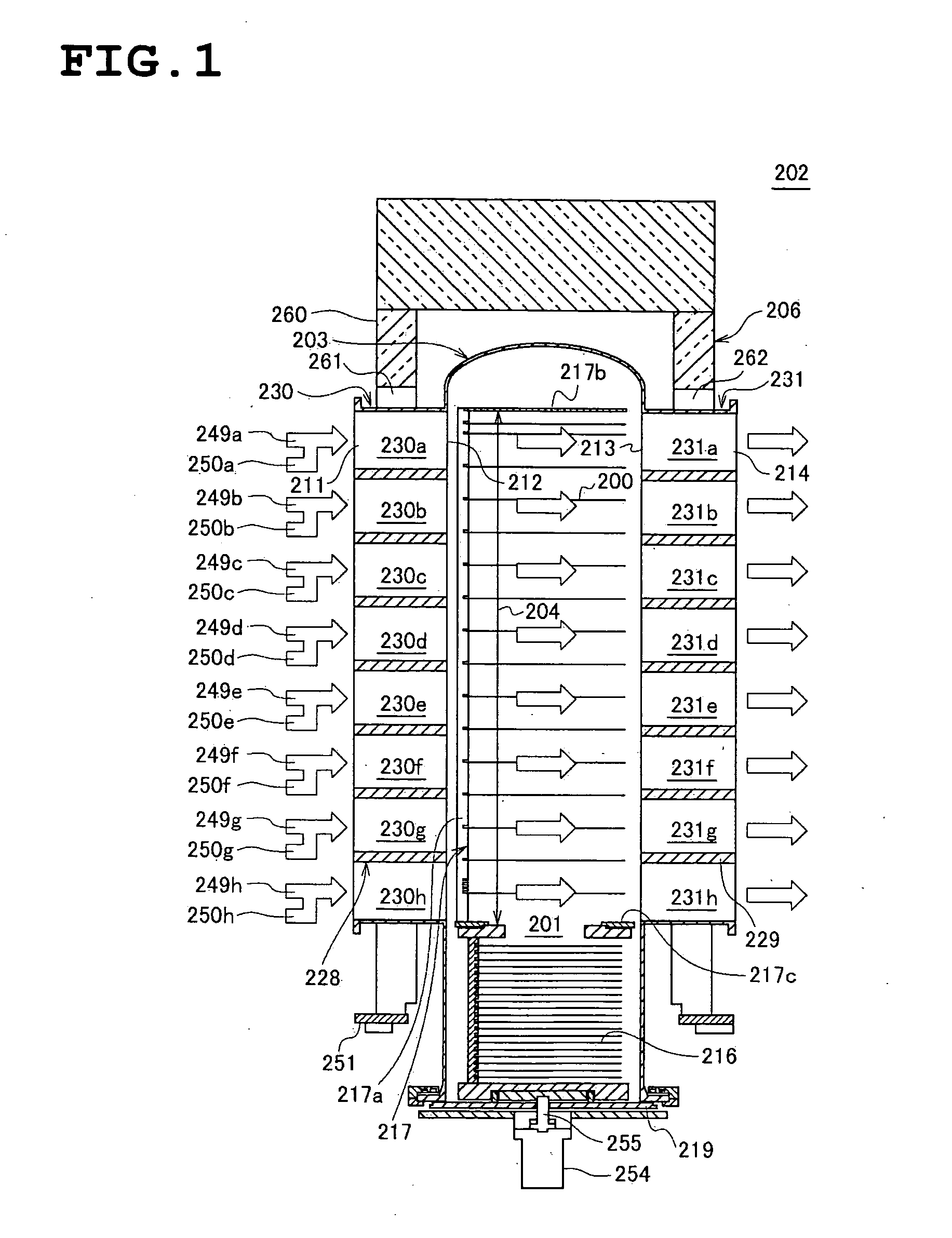
[0110]While the first embodiment described above describes, as shown in FIG. 3, a case in which a plurality of gas introduction partition portions 230a to 230h and gas exhaust partition portions 231a to 231h are integrally provided in a single gas inlet tube 230 and a single gas exhaust tube 231a as a result of these long, elliptically-shaped pipes being partitioned in the vertical direction by partition walls 228, 229, the present invention is not limited thereto.

[0111]For example, as in a first modification thereof shown in FIG. 4, on the basis of a plurality of gas inlet tubes 230 and gas exhaust tubes 231 of a cylindrical shape being arranged in rows in the vertical direction of the reaction tube 203 and joined by way of common flanges 232, 233, the plurality of gas introduction partition portions 230a to 230h and gas exhaust partition portions 2...

second embodiment

Modifications

[0164]The following range of modifications can be made to the second embodiment of the present invention described above.

>

[0165]While the embodiment described above describes an example in which the processing partition walls provided in the port describe a disc shape and are formed in a certain arrangement and number in the port, the shape, arrangement and number of these processing partition walls is not limited thereto.

>

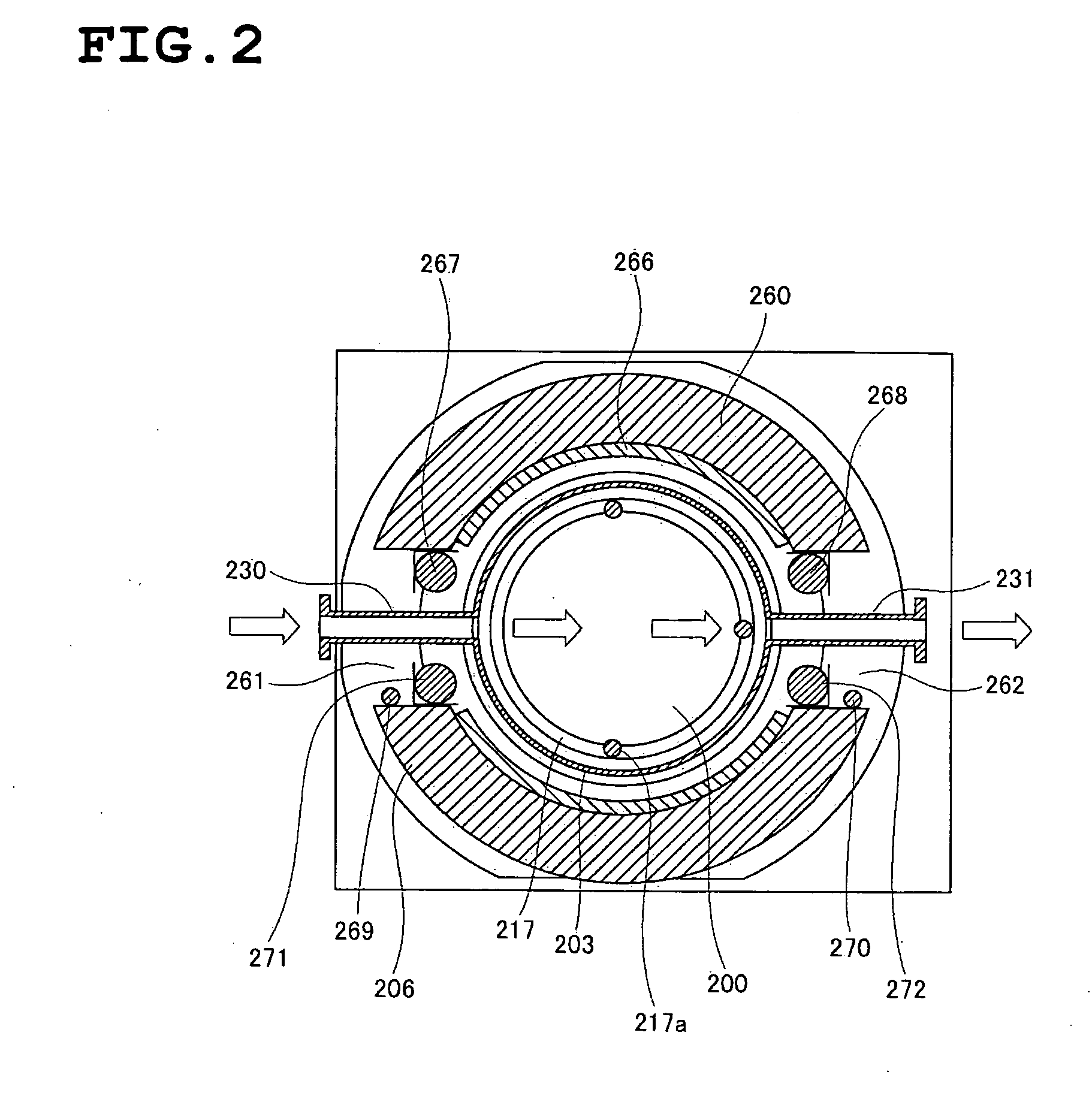
[0166]In addition, while the port 21 of the embodiment described above is integrated, an assembled body that is disassemblable into processing partition units may be adopted. For example, a port 217 formed as a laminate of port constituent elements may be adopted. The assembly of this port is based on a plurality of port constituent elements being disposed in an arrangement in which one port constituent element is placed on another port constituent element in sequence.

[0167]For example, as in a first modification shown in FIG. 26, the basic configurat...

example processing conditions

[0278]As an example of the processing conditions for processing wafers in the processing furnace of the embodiments for the film formation of a Si3N4 film includes a processing pressure of 30 Pa, the employment of dichlorosilane gas (SiH2Cl2) and ammonia gas (NH3) as the gas types, and a gas supply flow rate to the partition portions of SiH2Cl2 0.1 sccm and NH3 0.5 sccm may be employed. The conditions additionally include a processing temperature in the reaction tube 203 heated by the heater wire 266a of 760° C., a temperature in the gas inlet tube 230 heated by the gas inlet tube side wall heating body 267a of 300° C., and a temperature of the gas exhaust tube 231 heated by the gas exhaust tube side wall heating body 268a of 300° C.

[0279]The wafer processing is administered p with each of these respective processing conditions maintained to a constant value within a respective range thereof.


PUM

PropertyMeasurementUnit
Temperatureaaaaaaaaaa
Diameteraaaaaaaaaa
Areaaaaaaaaaaa

Abstract

A substrate processing apparatus that affords improved uniformity to in-plane wafer and interwafer film thickness of a large number of wafers on which a film is simultaneously formed, having: a reaction tube having in an interior thereof a processing chamber in which a plurality of substrates disposed in a direction perpendicular to a substrate processing surface can be processed; and a heating device provided to surround an outer circumference of the reaction tube, a gas inlet tube being provided on a side face of the reaction tube in a region for processing a substrate inside the reaction tube, so as to reach at least an outside of the heating device; and a gas spouting port being disposed in this gas inlet tube in a slit form so as to straddle at least a plurality of the substrates in a direction perpendicular to the substrate processing surface, for spouting gas from the gas inlet tube into the processing chamber.

Description

BACKGROUND OF THE INVENTION[0001]1. Field of the Invention[0002]The present invention relates to a substrate processing apparatus and method of manufacturing a semiconductor device, and more particularly to the effective utilization thereof in a substrate processing technology in which, in a process for manufacturing a semiconductor device, a thermochemical reaction is utilized to administer a desired processing such as the fabrication of an oxide film or metal film on a substrate such as a semiconductor wafer (hereinafter also referred to as a wafer).[0003]2. Description of the Related Art[0004]In a process for manufacturing a semiconductor device, vertical-type semiconductor manufacturing apparatuses are sometimes employed as substrate processing apparatuses for fabricating an oxide film or metal film on a wafer.[0005]Conventional vertical-type semiconductor manufacturing apparatuses of this type comprise a processing furnace configured from a reaction vessel and a heater in which...

Claims


Application Information

Patent Timeline
IPC IPC(8): C23C16/513H01L21/283C23C16/44
CPCC23C16/345C23C16/44C23C16/4584C23C16/45502C23C16/45519C23C16/4412
Inventor NAKASHIMA, SEIYOABURATANI, YUKINORI
Owner KOKUSA ELECTRIC CO LTD
Why Eureka
Try Eureka