Method For Manufacturing Of Electronics Package

a manufacturing method and electronic technology, applied in the manufacture of printed circuits, magnetic/electric field screening, cross-talk/noise/interference reduction, etc., can solve the problems of increased weight of electronic packages, reduced shielding efficiency, and time-consuming mounting

Inactive Publication Date: 2008-07-24
NOKIA CORP
View PDF10 Cites 23 Cited by
  • Summary
  • Abstract
  • Description
  • Claims
  • Application Information

AI Technical Summary

Benefits of technology

[0020]This embodiment allows removing the dielectric layer e.g. at the edge of an electronic component, such th...

Problems solved by technology

Such metal shielding cans are relatively expensive, need to be mounted in an additional process step in manufacturing, substantially increase the weight of the completed electronic package and also may cause thermal problems, as there may always be a certain amount of air trapped between the component and the shielding can which causes an unwished thermal isolation.
It can therefore be required to provide apertures in the shielding for removing heat from electronic components, which in turn reduces the shielding efficiency.
The mounting is time-expensive and can thus slow down the production process.
In case of soldering or gluing the conventional mounting of a shielding can also entail severe environmental issues due to the resulting waste and residues of hazardous substances used.
In small electronic devices there can also be issues with respect to the space needed inside the electronic device for accommo...

Method used


Image

  • Method For Manufacturing Of Electronics Package
  • Method For Manufacturing Of Electronics Package
  • Method For Manufacturing Of Electronics Package

Examples


Embodiment Construction

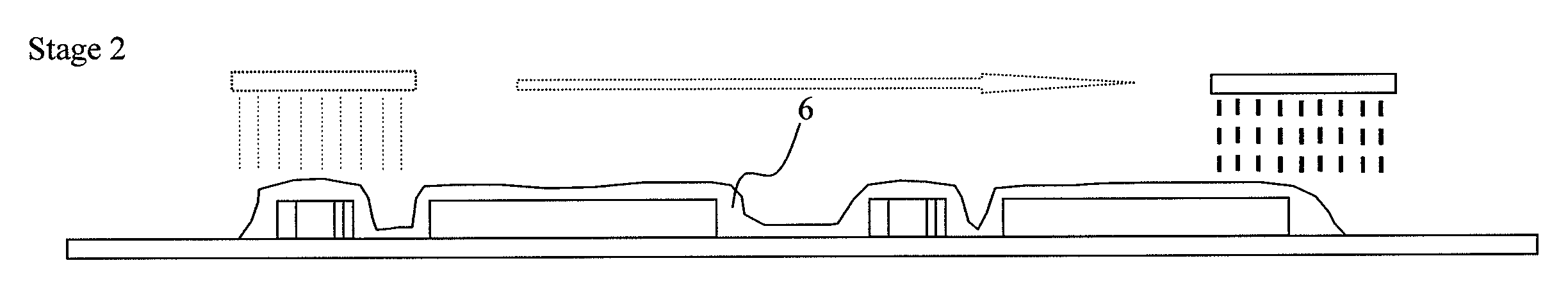
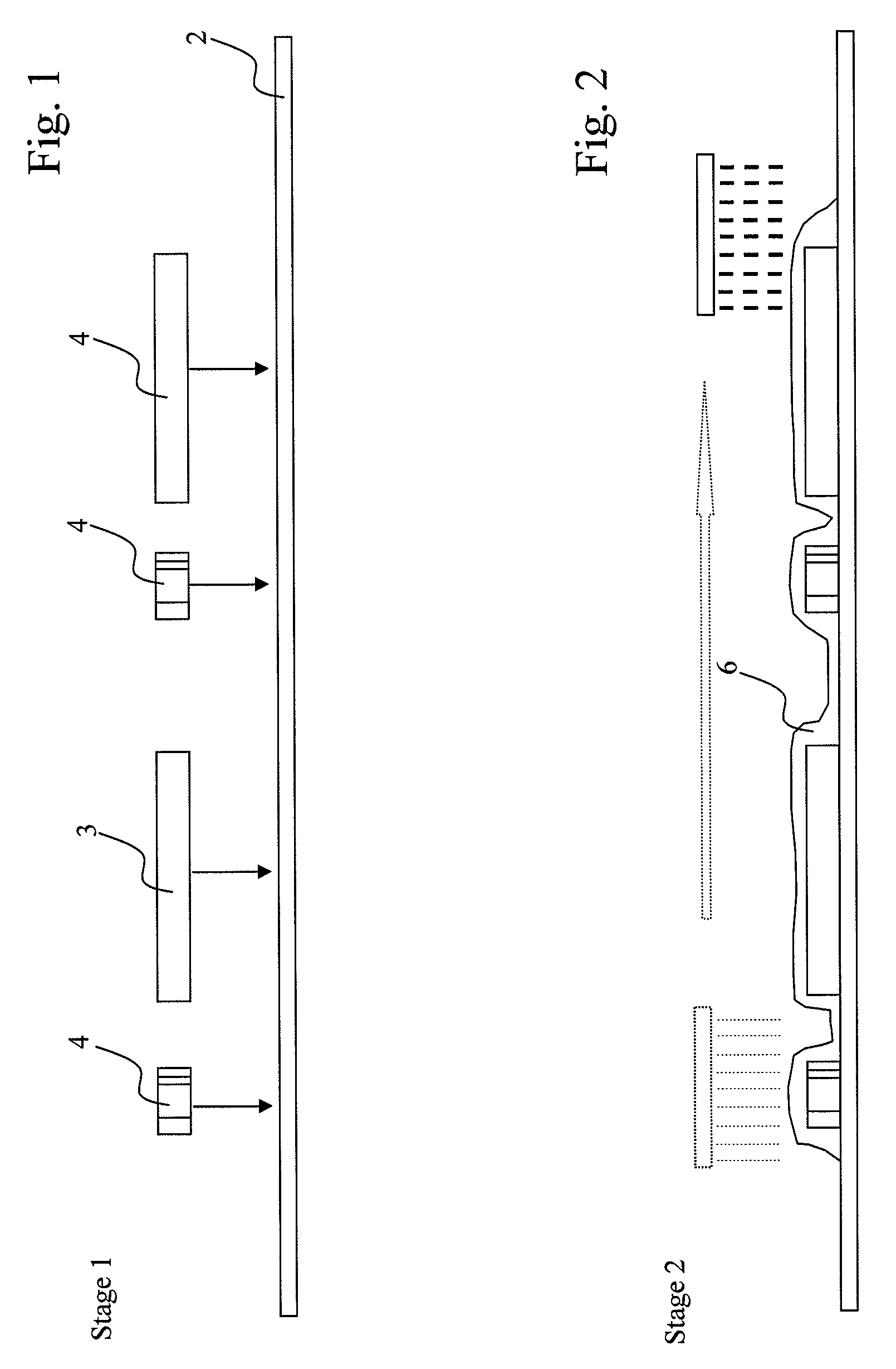
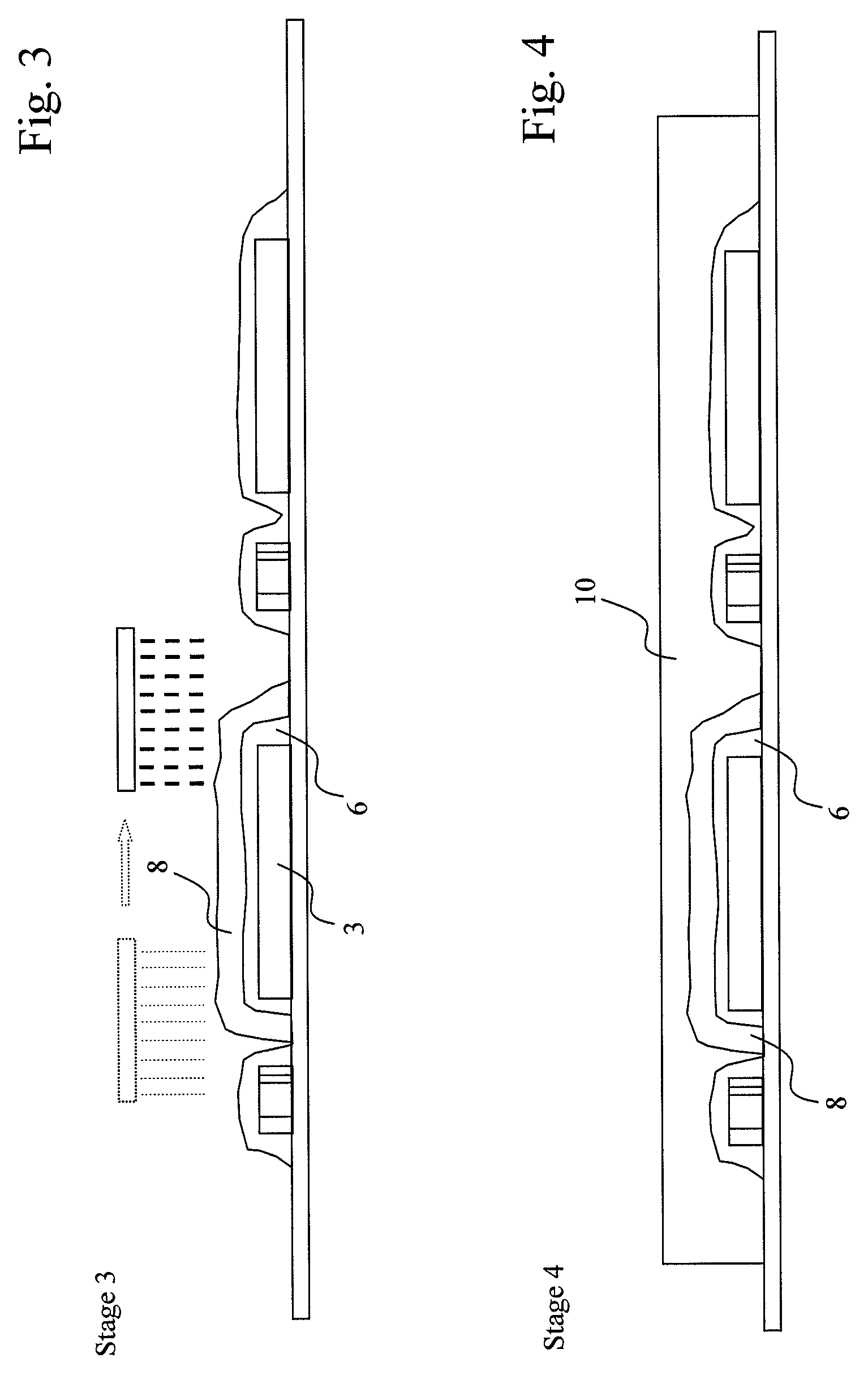
[0072]It is to be noted that the following description of exemplary embodiments will focus on a particular deposition technique, that is, deposition of layers by inkjet printing. However, the invention is not restricted to inkjet printing but also includes applying layers by any other suitable deposition method such as maskless mesoscale material deposition, M3D.

[0073]Furthermore it will be appreciated that common steps that do not constitute part of the invention themselves, such as curing of applied layers, will not be described in detail in the following. For example curing can be performed by applying heat, laser, ultra violet, UV radiation and also by chemical reaction.

[0074]Embodiments of the invention can help to improve the Electro-Magnetic Interference (EMI) properties of printed circuit modules or electronic packages, respectively. It makes possible to achieve greater integration and decreases the size of electronics packages (i.e. make them lighter, thinner and smaller wi...


PUM


Abstract

A method for manufacturing an electronics package is provided in which a carrier is provided, at least one electronic component is placed on the carrier and a base layer is then deposited on the electronic component(s). The base layer may include a dielectric layer binding the electronic component(s) to the carrier and providing an adhesive surface for further layers. Alternatively, the base layer may include an electrically conductive layer binding the electronic component(s) to the carrier and providing electromagnetic shielding for the electronic component(s) and an adhesive surface for further layers. A corresponding shield and a computer-readable medium for storing instructions for instructing a computer to perform the manufacturing method are also provided.

Description

[0001]Embodiments of the invention relate in general to the manufacturing of electronics packages, and in particular to the provision of electronics packages with improved electromagnetic shielding, adhesion and fixation of components.BACKGROUND[0002]Electromagnetic shielding is used in electronic devices to shield electromagnetic interferences from sensitive electronic devices or circuits, or vice versa. An example of such electronic circuits is a Wireless Local Area Network WLAN transceiver or cellular RF transceiver. To achieve the shielding, the electromagnetic interferences are shielded by providing an electrically conductive enclosure around the device or circuit to be protected.[0003]Conventionally electromagnetic shielding is performed by providing casings or “cans” of conductive material around the circuits to be protected. In the production of electronic devices these cans must be arranged on the components to be protected and then affixed thereto, e.g. by soldering.[0004]...

Claims


Application Information

Patent Timeline
IPC IPC(8): H01L21/00H01L21/3205
CPCH01L21/56H01L21/568H01L2924/19105H05K1/0218H05K1/185H01L2224/49171H05K2203/013H05K2203/016H05K2203/1316H05K2203/1469H05K9/0024H01L2924/181H01L2224/05554H01L2924/00012
Inventor MOLKKARI, PETRIMANSIKKAMAKI, PAULIINAMANTYSALO, MATTIMIETTINEN, JANIVALTANEN, JANI
Owner NOKIA CORP
Why Eureka
Try Eureka