Substrate and semiconductor device using the same

a technology of semiconductor devices and substrates, applied in the direction of printed circuit manufacturing, printed circuit aspects, basic electric elements, etc., can solve the problems of disadvantageous lowering reliability of semiconductor devices, migration on the side, etc., and achieve the effect of improving the reliability of semiconductor devices and improving the productivity of them

Inactive Publication Date: 2008-07-31
PANASONIC CORP
View PDF5 Cites 10 Cited by
  • Summary
  • Abstract
  • Description
  • Claims
  • Application Information

AI Technical Summary

Benefits of technology

[0013]To solve such conventional problems, an object of the present invention is to provide a substrate that can improve the reliability and productivity of semiconductor devices, and a semiconductor device using such a substrate.
[0016]According to the present invention, as described above, recesses are formed in the peripheral portion of each semiconductor package substrate in the substrate, and since the warpage of each semiconductor package substrate can be relieved by the recesses and the warpage of the entire substrate can be reduced, the mounted quality, when a semiconductor chip is mounted on each semiconductor package substrate in the subsequent steps of forming the substrate, can be improved.
[0017]Since the internal conductor portions are not exposed on the side of the semiconductor device formed with resin molding performed after mounting semiconductor chips on each semiconductor package substrate as in the conventional way, the occurrence of short-circuiting and migration between conductors can be avoided; and since the side of the semiconductor device is only the interface between the molding resin having high adhesiveness and the base material of the semiconductor package substrate, the invasion of moisture into the semiconductor device from outside can also be minimized.
[0018]Thereby, the reliability of the semiconductor device can be improved, and the expansion of applications, such as on-board systems used in a harsh environment, can be realized.
[0020]As a result, the reliability of the semiconductor device can be improved, and the productivity thereof can also be improved.

Problems solved by technology

Further, the deposition of impurity ions and the moisture absorption of the semiconductor device may cause migration on the side.
Therefore, the semiconductor device has disadvantageously lowered reliability.

Method used


Image

  • Substrate and semiconductor device using the same
  • Substrate and semiconductor device using the same
  • Substrate and semiconductor device using the same

Examples


Embodiment Construction

[0036]A substrate and a semiconductor device using such a substrate according to an embodiment of the present invention will be specifically described referring to the drawings.

[0037]The substrate according to the embodiment of the present invention will be described.

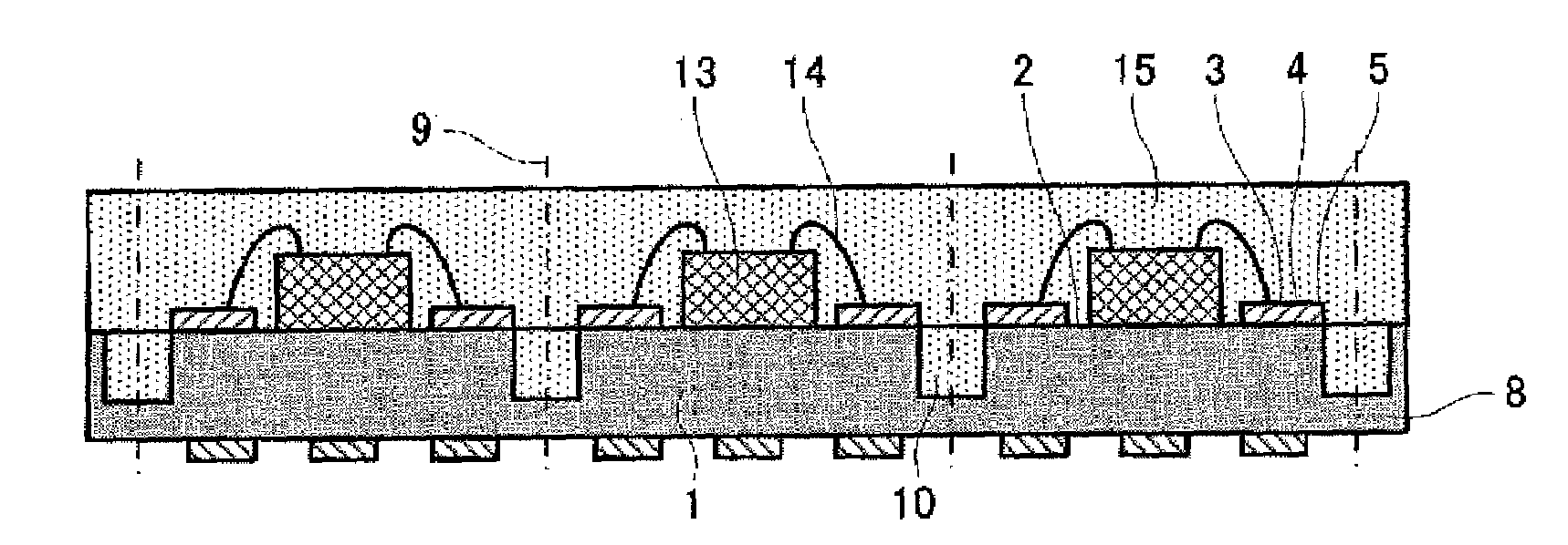
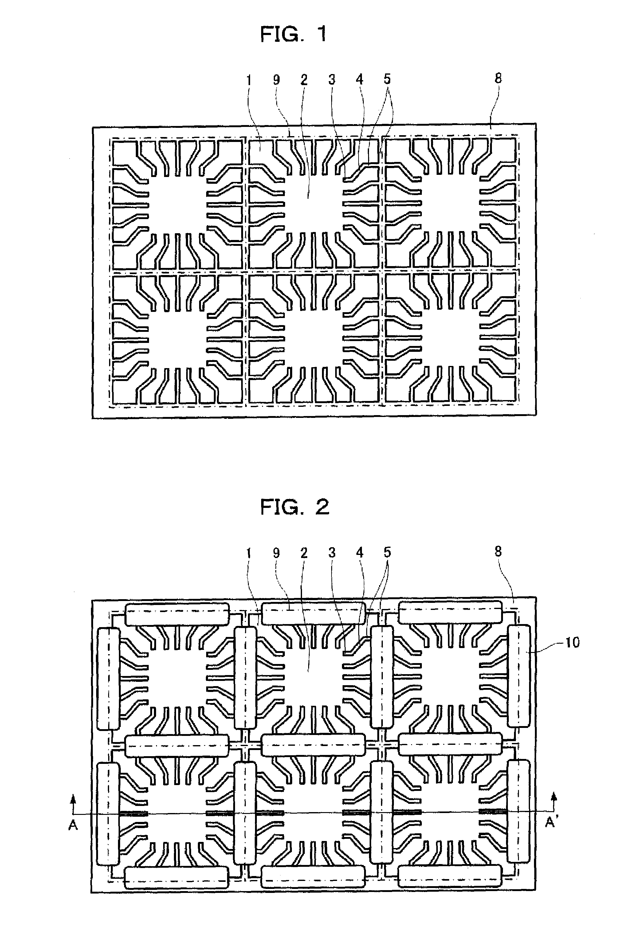
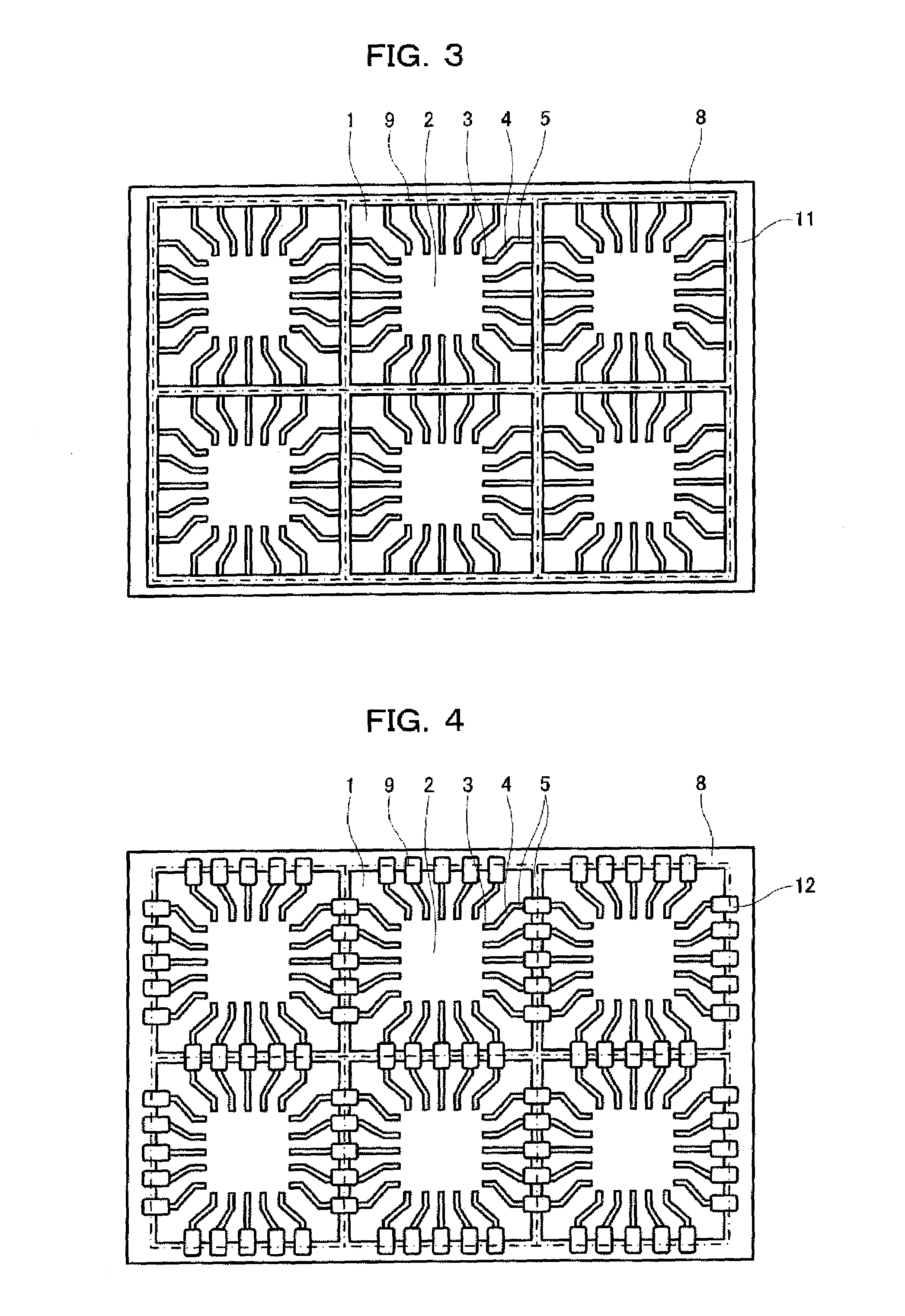
[0038]FIG. 1 is a top view showing a state where a wiring pattern is formed on the substrate according to the embodiment of the present invention; FIG. 2 is a top view showing a state where trench-shaped recesses are formed on the peripheral portion of each semiconductor package substrate only in a region of wirings for plating in the substrate according to the embodiment; FIG. 3 is a top view showing a state where ring-shaped recesses are formed on the entire peripheral portion of each semiconductor package substrate in the substrate according to the embodiment; and FIG. 4 is a top view showing a state where independent recesses for each wiring for plating are formed on the peripheral portion of each semiconductor pack...


PUM


Abstract

According to the present invention, a plurality of semiconductor devices having semiconductor chips 13 molded on a semiconductor package substrate 1 by a molding resin 15 can be manufactured by forming recesses 10 around each semiconductor package substrate 1 composing a substrate 8 for a BGA package, and in the state where a molding resin 15 is filled on the substrate 8 including the recesses 10 for resin molding, cutting the substrate 8 and the molding resin 15 along partition lines 9.

Description

FIELD OF THE INVENTION[0001]The present invention relates to a substrate consisting of a plurality of semiconductor package substrates on which semiconductor chips are mounted used in a BGA package and the like, and a semiconductor device using such a substrate.BACKGROUND OF THE INVENTION[0002]In recent years, in order to cope with the size reduction of electronic devices such as mobile communication apparatuses, size reduction and high integration are also required in semiconductor devices. As the high functionality and multi-functionality of electronic devices have advanced, BGA packages and LGA packages for semiconductor devices whose external terminals tend to have a large number of pins and are disposed on the bottom surface of the package in an area array form are frequently used.[0003]Such semiconductor devices are obtained, for example, in a state where semiconductor chips are molded with a molding resin on each semiconductor package substrate composing a substrate for a BGA...

Claims


Application Information

Patent Timeline
Patent Type & Authority Applications(United States)
IPC IPC(8): H01L23/48
CPCH01L21/561H01L2924/01006H01L23/3121H01L24/45H01L24/48H01L24/97H01L2224/45015H01L2224/45124H01L2224/45144H01L2224/45147H01L2224/48091H01L2224/48227H01L2224/484H01L2224/48599H01L2224/48699H01L2224/85447H01L2224/97H01L2924/01002H01L2924/01004H01L2924/01005H01L2924/01013H01L2924/01028H01L2924/01029H01L2924/01033H01L2924/01078H01L2924/01079H01L2924/01082H01L2924/15159H01L2924/20751H01L2924/20752H05K3/0052H05K3/284H05K2201/09036H05K2201/0909H01L23/13H01L2924/00014H01L2224/85H01L2924/181H01L2224/48847H01L2224/48647H01L2224/48747H01L2924/00H01L2924/00012
Inventor FUJIMOTO, HIROAKIIMAZU, KENICHI
Owner PANASONIC CORP
Why Eureka
Try Eureka