Solid-state image capturing apparatus, method for manufacturing same, and electronic information device

a technology of solid-state image and capturing apparatus, which is applied in the direction of radio frequency controlled devices, television system scanning details, television systems, etc., can solve the problems of image deterioration and increase in residual images, and achieve the effect of suppressing fluctuations in device characteristics caused by processing variations and improving the reliability and productivity of solid-state image capturing apparatus

Active Publication Date: 2012-02-14
SMARTSENS TECH (SHANGHAI) CO LTD
View PDF11 Cites 0 Cited by
  • Summary
  • Abstract
  • Description
  • Claims
  • Application Information

AI Technical Summary

Benefits of technology

[0013]As described above, in the manufacturing method of the solid-state image capturing apparatus disclosed in Cited Reference 1, the ion implantation angle is set based on the positional relationship between the edge of the opening of the transfer electrode and the edge of the readout gate region, and an impurity concentration is adjusted in the region between the p-type diffusion layer 9 in the surface portion of the sensor region and the readout gate region 30 when ions are implanted into the surface layer portion of the sensor region via the opening of the transfer electrode. In other words, after a readout gate electrode is fabricated, and prior to the formation of an interlayer insulation film (sidewalls) thereon, the ion implantation angle is determined, and a surface P+ layer for suppressing dark voltage is formed. Thereby, fluctuations in the characteristics of the device caused by variations in processing are suppressed, which achieves to improve the reliability and productivity of the solid-state image capturing apparatus.

Problems solved by technology

As a result, problems such as an increase in a residual image and image deterioration occur.

Method used


Image

  • Solid-state image capturing apparatus, method for manufacturing same, and electronic information device
  • Solid-state image capturing apparatus, method for manufacturing same, and electronic information device
  • Solid-state image capturing apparatus, method for manufacturing same, and electronic information device

Examples


embodiment 1

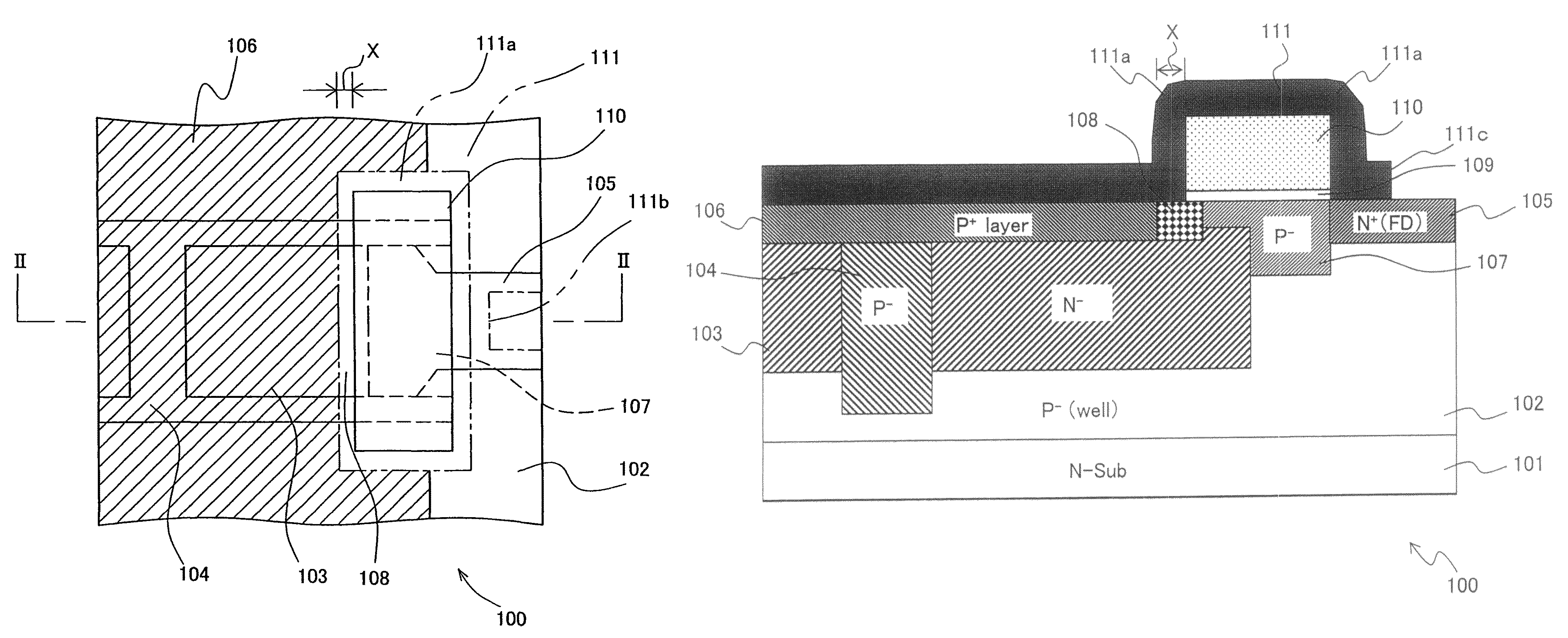
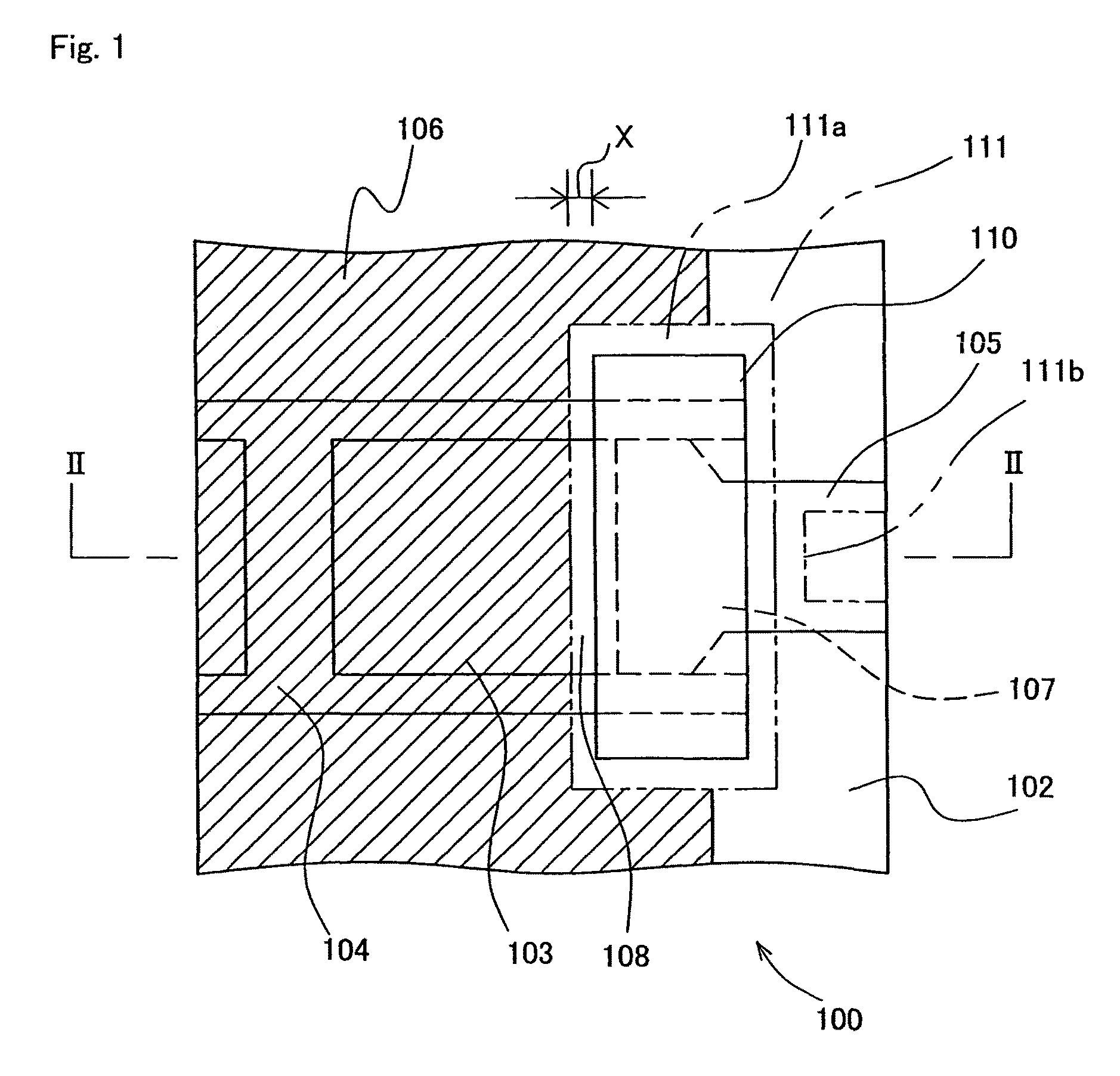
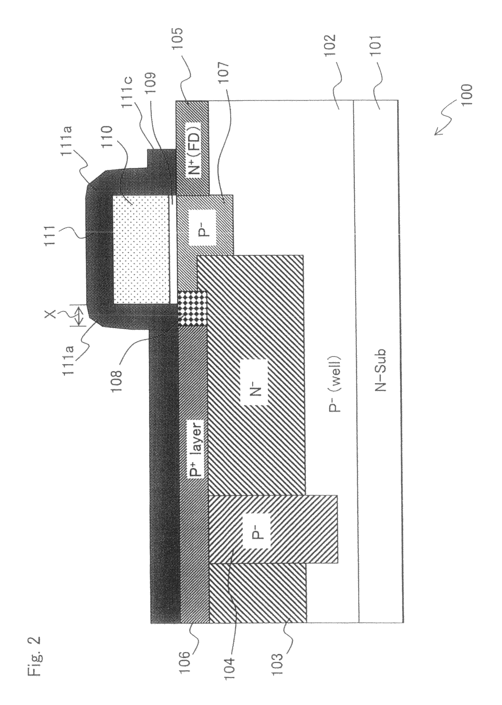
[0081]FIG. 1 is a plan view describing a solid-state image capturing apparatus according to Embodiment 1 of the present invention, illustrating an essential part layout of pixels constituting the solid-state image capturing apparatus. FIG. 2 is across sectional view describing the solid-state image capturing apparatus according to Embodiment 1, illustrating a structure of the cross section along the line II-II of FIG. 1.

[0082]A solid-state image capturing apparatus 100 of Embodiment 1 includes, a P− well 102 formed on an N type silicon substrate (N-Sub) 101. In the P− well 102, an N− type conductivity PD diffusion layer 103, which constitutes a photoelectric conversion region (hereinafter, also referred to as “light-receiving section or photodiode”) is arranged in a matrix and an N+ type conductivity FD diffusion layer 105, which constitutes an electric charge accumulation region (FD), is formed in such a manner to oppose to the PD diffusion layer 103. Also, between the diffusion la...

embodiment 2

[0103]FIG. 7 is a plan view describing a solid-state image capturing apparatus according to Embodiment 2 of the present invention, illustrating a layout of an essential part of pixels constituting the solid-state image capturing apparatus. FIG. 8 is a cross sectional view describing the solid-state image capturing apparatus according to Embodiment 2, illustrating a structure of the cross section along the line XIII-XIII of FIG. 7.

[0104]The solid-state image capturing apparatus 100a according to Embodiment 2 has a structure where the CVD film 111, which is formed on the readout gate electrode 110 in the solid-state image capturing apparatus 100 according to Embodiment 1 in a manner to reflect the height difference thereunder, is etched away such that only the portions of the CVD film 111 adjacent to the side surface portions of the readout gate electrode 110 remain. The solid-state image capturing apparatus 100a according to Embodiment 2 is different from the solid-state image captur...

embodiment 3

[0120]FIG. 10 is a block diagram schematically illustrating an exemplary structure of an electronic information device of Embodiment 3 of the present invention, including at least one of the solid-state image capturing apparatus according to Embodiments 1 and 2 of the present invention in an image capturing section thereof.

[0121]In FIG. 10, an electronic information device 90 according to Embodiment 3 of the present invention includes: the solid-state image capturing apparatus according to either of Embodiments 1 and 2 of the present invention as an image capturing section 91 for capturing an image of a subject, and the electronic information device 90 further includes at least one of: a memory section 92 (e.g., recording media) for data-recording a high-quality image data obtained by using at least one of the solid-state image capturing apparatus according to Embodiments 1 and 2 in an image capturing section, after a predetermined signal process is performed on the image data for r...


PUM


Abstract

A solid-state image capturing apparatus according to the present invention includes: a plurality of photoelectric conversion sections; a charge accumulation section; and a charge readout section, the apparatus further includes: a semiconductor substrate including a plurality of diffusion layers formed thereabove, the diffusion layers constituting the photoelectric conversion sections, the charge accumulation section and the charge readout section; a readout gate electrode formed above the semiconductor substrate and constituting the charge readout section; an insulation sidewall formed on a side surface of the readout gate electrode; and a surface diffusion layer constituting the photoelectric conversion sections, which is positioned in a self-aligning manner with respect to the readout gate electrode by the insulation sidewall.

Description

[0001]This nonprovisional application claims priority under 35 U.S.C. §119(a) to Patent Application No. 2008-321522 filed in Japan on Dec. 17, 2008, the entire contents of which are hereby incorporated by reference.BACKGROUND OF THE INVENTION[0002]1. Field of the Invention[0003]The present invention is related to: a solid-state image capturing apparatus; a method for manufacturing the solid-state image capturing apparatus; and an electronic information device, and more specifically, a solid-state image capturing apparatus including light-receiving sections each constituted of an embedded photodiode and capable of reading out a signal charge from the light-receiving section in low voltage drive and realizing low-noise and high-definition images, a method for manufacturing the solid-state image capturing apparatus, and an electronic information device including the solid-state image capturing apparatus.[0004]2. Description of the Related Art[0005]Conventionally, a solid-state image ca...

Claims


Application Information

Patent Timeline
Patent Type & Authority Patents(United States)
IPC IPC(8): H04N3/14H01L21/339H01L21/00H01L27/148H04N5/335H01L27/146
CPCH01L27/14607H01L27/14612H01L27/1463H01L27/146
Inventor MUTOH, AKIYOSHI
Owner SMARTSENS TECH (SHANGHAI) CO LTD
Why Eureka
Try Eureka