Eureka AIR delivers breakthrough ideas for toughest innovation challenges, trusted by R&D personnel around the world.

Microelectronics Package and Method

Inactive Publication Date: 2008-07-31
GENERAL LED
View PDF7 Cites 11 Cited by
  • Summary
  • Abstract
  • Description
  • Claims
  • Application Information

AI Technical Summary

Benefits of technology

[0005]The present invention provides a method of packaging microelectronic devices, such as silicon chips and electrical components, in a way that produces flat small and lightweight packages. Accordingly, the principal object of the present invention is to provide a method and device that solves the above disadvantage of the prior art. Therefore the present invention provides a method for micropackaging LED diodes on a flexible substrate, and micropackages including a flexible substrate that will not suffer the disadvantages of the prior art and pop-off or lose connections when the substrate is flexed.
[0007]The embedding of the device or component in the flexible substrate will enhance the procedure for making lightwires that are planar and small and thin.

Problems solved by technology

Various techniques have been proposed for packaging microelectronics and electrical devices, but none offer a planarized package, or the capability to make small and flat packages, such that mass production can take place more effectively, and the resulting products are reduced in size and weight.
Since the LED component is a rigid chip, if surface mounted on a flexible substrate, there is a danger that the component or one or more of the connections to the flexible substrate will pop-off or disconnect when the substrate is flexed.

Method used


Image

  • Microelectronics Package and Method
  • Microelectronics Package and Method
  • Microelectronics Package and Method

Examples


Embodiment Construction

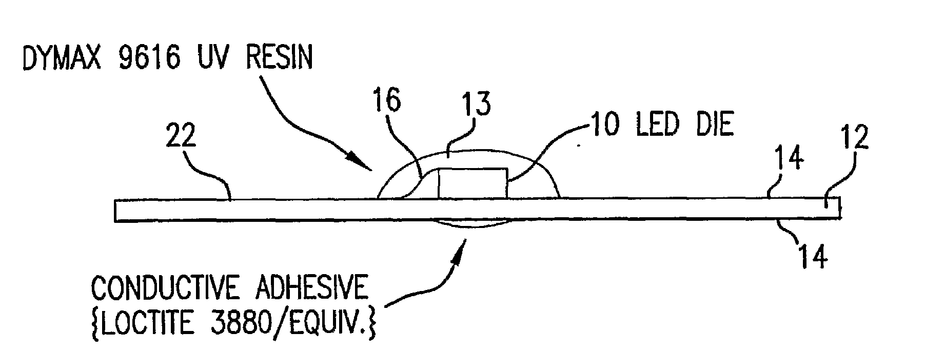
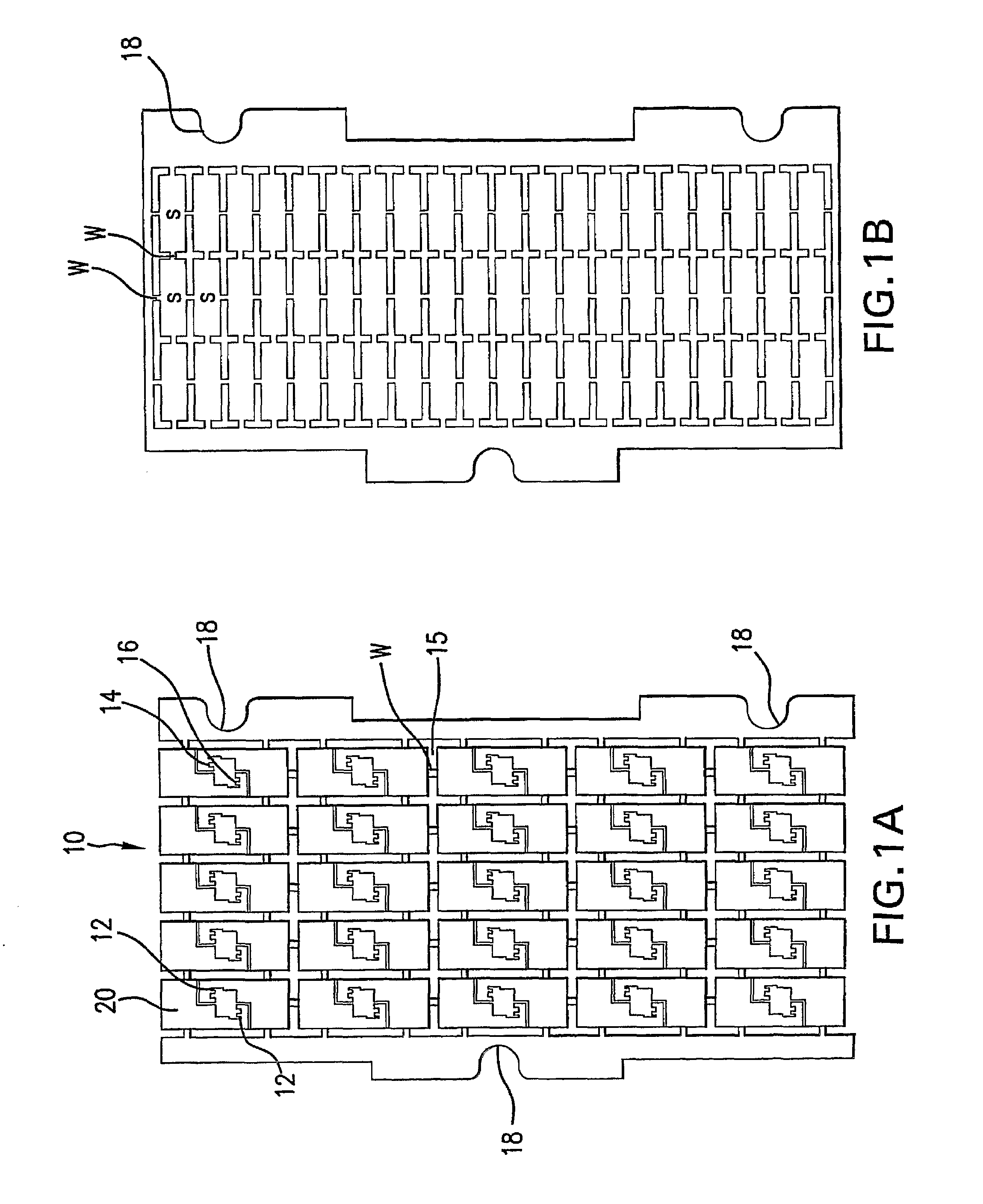
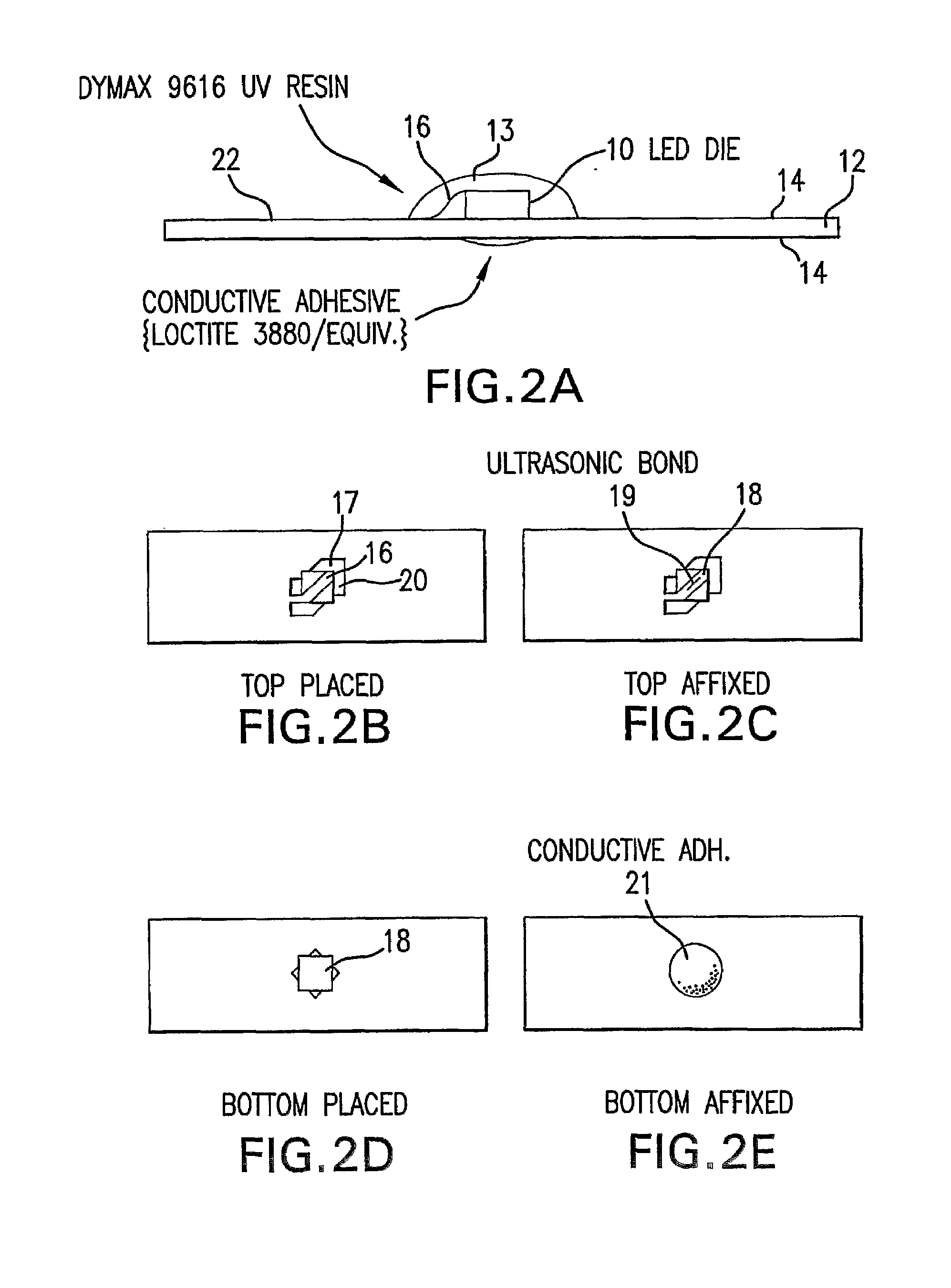
[0022]Unique packaging of microelectronic components is shown in FIGS. 1A and 1B. There is shown a flat panel 10 composed of plastic with copper films top and bottom. By known photo imaging and lithographic processing the copper films are removed in selected areas to reveal a plurality of bare plastic areas on one side and configured on the other side, shown in FIG. 1A, the copper film is formed into two electrodes 12 per site 20 and two contacts 14 per site to be bonded with diodes 16 positioned in the sites, as shown in U.S. Pat. No. 6,956,182 issued Oct. 18, 2005 to the same inventor, said patent being incorporated herein by reference in its entirety. The sites 20 are defined by cutouts 15 punched in the substrate leaving webs W. The panel 10 is provided with indexing cutouts 18 for positioning in a pick and place machine. The diodes can be of any type, e.g. LED diodes, photo diodes or other types. The arrangement of a micropackage, comprising an array of sites as shown in FIGS. ...


PUM


Abstract

A lightwire segment in the form of an elongated substrate frame composed of a flat flexible thin elongated sheet of plastic dielectric material having a copper film laminated on at least one side; a plurality of cavities longitudinally spaced along the elongated substrate, a LED diode having first and second contacts embedded in each of the cavities of the substrate; the copper film on one side of the substrate defining two interconnects separated by a dielectric space, one interconnect having a tab bonded to the first contact of each LED diode, and the other interconnect having a tab bonded to the second contact of each LED diode. A lightwire made from a plurality of segments that are bonded together in series or parallel. A micropackage made from a substrate frame composed of a flat flexible thin sheet of plastic dielectric material having a copper film laminated on one side defining rows and columns of component sites separated from one another by thin webs to be readily detached from the substrate frame. The micropackage has indexing elements to position the substrate frame relative to a machine that can pick the component sites out of the frame. Each component site defines a cavity formed in the substrate, and the copper film laminated on the substrate defines two separated interconnects, each having a tab extending into the cavity formed in the substrate. An electrical component having contacts is positioned in the cavity and its contacts are bonded to the tabs.

Description

BACKGROUND OF THE INVENTION[0001]1. Field of the Invention[0002]The invention relates to a method for micropackaging small chips and other electrical components and the resulting micropackage. More particularly, the invention relates to a method for micropackaging small chips and other electrical components and forming a lightwire, wherein LED diodes are embedded in a flexible plastic substrate and further relates to a micropackage that has an array of LED diodes embedded in an elongated flexible plastic substrate.[0003]2. Prior Art[0004]Various techniques have been proposed for packaging microelectronics and electrical devices, but none offer a planarized package, or the capability to make small and flat packages, such that mass production can take place more effectively, and the resulting products are reduced in size and weight. In the past, LED diodes have been package by surface mounting the dies or chips using wire bonding or flip chip technology. Since the LED component is a r...

Claims


Application Information

Patent Timeline
IPC IPC(8): H01L23/52H02H1/00H05B37/00H01J9/00H01L33/48
CPCF21S4/003F21Y2101/02H01L33/48H05K1/184H05K1/189H05K3/0052H05K2201/0397H01L2924/0002H05K2201/09063H05K2201/0909H05K2201/10106H01L2924/00F21S4/20F21Y2115/10
Inventor GREGORY, JOHN
Owner GENERAL LED
Why Eureka
Eureka Blog
Learn More