Semiconductor transistor and fabrication method thereof

a technology of semiconductors and transistors, applied in the field of semiconductor transistors, can solve the problems of reducing the gate length, affecting the stability of the minimum voltage, and and the most pronounced effect of the gate length reduction is the loss of gate electrode control

Active Publication Date: 2021-08-05
UNITED SEMICONDUCTOR (XIAMEN) CO LTD
View PDF0 Cites 0 Cited by
  • Summary
  • Abstract
  • Description
  • Claims
  • Application Information

AI Technical Summary

Benefits of technology

[0005]One object of the present invention is to provide an improved semiconductor transistor and a manufacturing method thereof, which can solve the above-mentioned shortcomings and disadvantages of the prior art.

Problems solved by technology

However, one of the most pronounced effects occurs due to the gate length reduction is the loss of gate electrode control which is sometimes referred to as threshold (VT) roll-off.
However, due to the diffusion of the implanted dopants with the above-mentioned threshold adjustment ion implantation process, a Gauss function distribution is formed near the surface of the silicon substrate, and it is difficult to achieve a uniform dopant concentration distribution.
Therefore, the prior art cannot effectively control the instability phenomenon of the minimum voltage (Vmin) of the device caused by the leakage of the device.

Method used


Image

  • Semiconductor transistor and fabrication method thereof
  • Semiconductor transistor and fabrication method thereof
  • Semiconductor transistor and fabrication method thereof

Examples


Embodiment Construction

[0031]In the following detailed description of the disclosure, reference is made to the accompanying drawings, which form a part hereof, and in which is shown, by way of illustration, specific embodiments in which the invention may be practiced. These embodiments are described in sufficient detail to enable those skilled in the art to practice the invention.

[0032]Other embodiments may be utilized and structural, logical, and electrical changes may be made without departing from the scope of the present invention. Therefore, the following detailed description is not to be considered as limiting, but the embodiments included herein are defined by the scope of the accompanying claims.

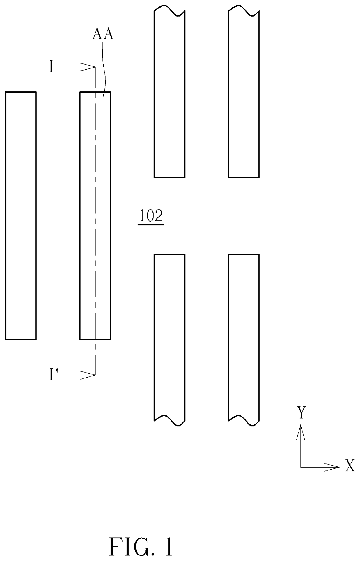
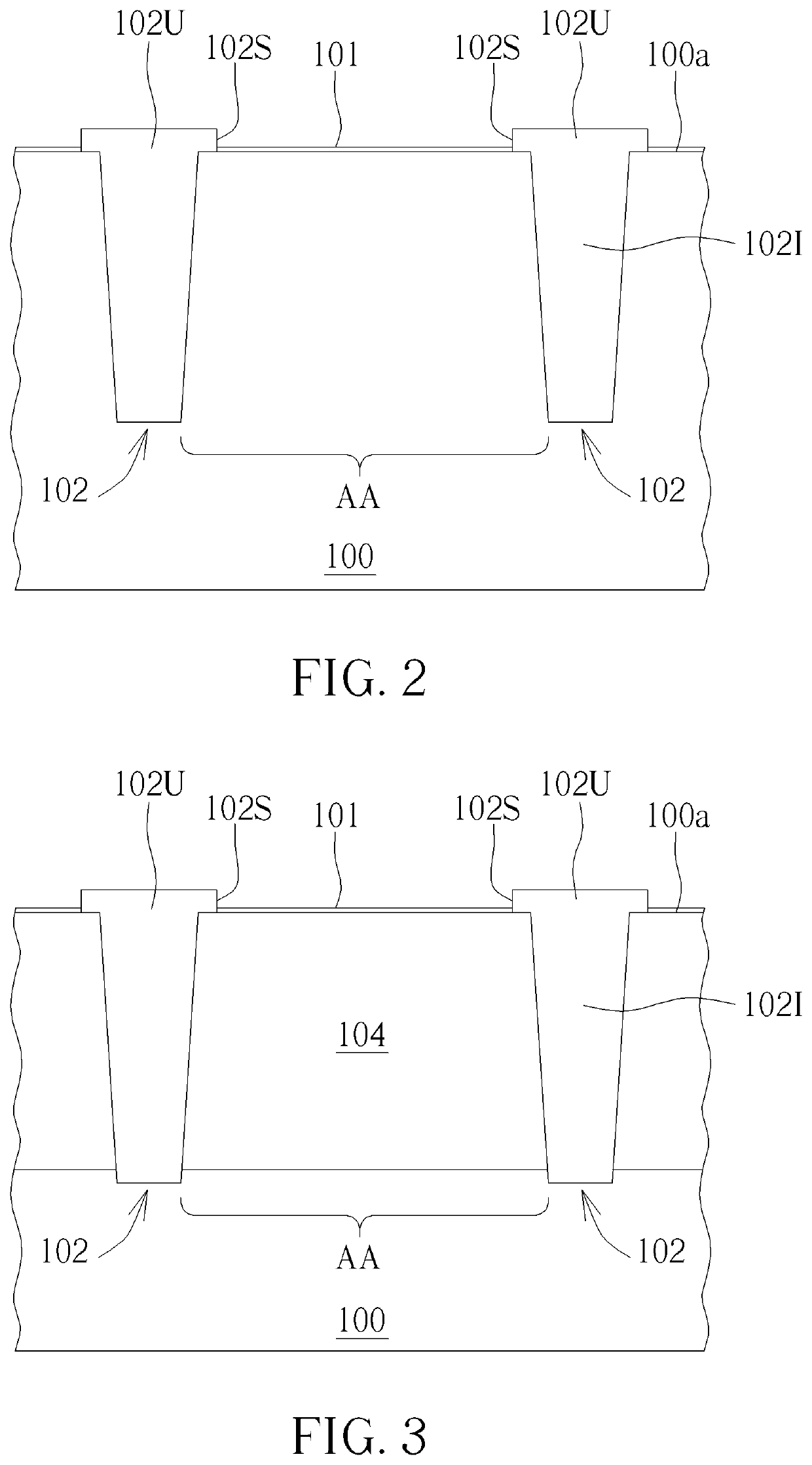
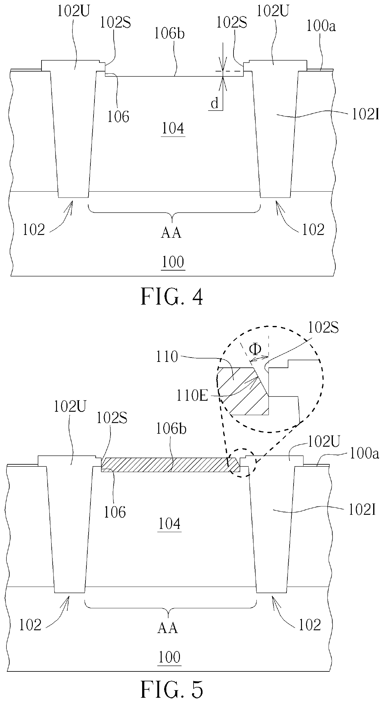
[0033]Please refer to FIG. 1 to FIG. 9, which are schematic diagrams of a method for fabricating a semiconductor transistor according to an embodiment of the present invention, wherein FIG. 1 and FIG. 7 illustrate partial layout diagrams of transistor devices, and FIGS. 2 to 6 and FIG. 9 are schematic cros...


PUM

PropertyMeasurementUnit
angleaaaaaaaaaa
thicknessaaaaaaaaaa
thicknessaaaaaaaaaa

Abstract

A semiconductor transistor is formed on a substrate of a first conductivity type. The substrate has a main surface. An ion well of the second conductivity type is disposed in the substrate. A source region and a drain region spaced apart from the source region are disposed within the ion well. The source region and the drain region have the first conductivity type. An epitaxial channel layer of the first conductivity type is grown from the main surface of the substrate and is disposed between the source region and the drain region. A gate is disposed on the epitaxial channel layer. A gate dielectric layer is disposed between gate and the epitaxial channel layer.

Description

BACKGROUND OF THE INVENTION1. Field of the Invention[0001]The present invention relates to the field of semiconductor technology, and in particular, to an improved semiconductor transistor and a method for manufacturing the same.2. Description of the Prior Art[0002]As known in the art, a MOSFET device includes a pair of source / drain regions formed on a surface of a silicon substrate, a gate oxide film formed on the substrate between the source / drain regions, and a gate electrode formed on the surface of the gate oxide film. The surface area of the substrate between the source region and the drain region is defined as a channel region. The length of the channel region is the distance between the source / drain regions, which is typically somewhat shorter than the gate length.[0003]In order to increase the speed of the MOS device, there exists a continuing trend of scaling-down the structure to smaller sizes. One of the ways of scaling is by reducing the length of the gate. However, one...

Claims


Application Information

Patent Timeline
Patent Type & Authority Applications(United States)
IPC IPC(8): H01L29/10H01L29/161H01L29/66H01L21/762
CPCH01L29/1033H01L21/76224H01L29/66477H01L29/161H01L29/78H01L29/66409H01L29/0684H01L29/66636
Inventor LIU, SHENG-HSUHUANG, SHIH-HSIENTAN, WEN YI
Owner UNITED SEMICONDUCTOR (XIAMEN) CO LTD
Why Eureka
Try Eureka