Semiconductor device

a technology of semiconductor devices and semiconductors, applied in the field of semiconductor devices, can solve problems such as deterioration of components and temperature increas

Active Publication Date: 2008-07-31
ROHM CO LTD
View PDF6 Cites 29 Cited by
  • Summary
  • Abstract
  • Description
  • Claims
  • Application Information

AI Technical Summary

Benefits of technology

[0025]With this arrangement, the thermal terminal is connected to the ground electrode on the mount board when the semiconductor device is mounted on the mount board. The provision of the thermal terminal makes it possible to electrically connect the semiconductor chip to the ground electrode via the island, the heat conduction portion, the thermal pad and the thermal terminal. As a result, a rear surface of the semiconductor chip is kept at a ground potential when the semiconductor device is mounted on the mount board. Therefore, a semiconductor chip formed with a power IC and operative with its rear surface grounded may be employed as the semiconductor chip. In this case, proper operation of the semiconductor chip (e.g., proper operation of the power IC) is ensured. Since the thermal terminal is connected to the ground electrode, the heat transferred to the thermal pad is released to the mount board through the thermal terminal.

Problems solved by technology

A recent trend toward the multi-functionality of the semiconductor chip has presented problems associated with a temperature increase due to heat generated by the semiconductor chip.
If the heat generated by the semiconductor chip remains in the semiconductor device (in the resin package), for example, inconveniences such as deterioration of the components and malfunction of the semiconductor chip may result.

Method used


Image

  • Semiconductor device
  • Semiconductor device
  • Semiconductor device

Examples


Embodiment Construction

[0037]Embodiments of the present invention will hereinafter be described in detail with reference to the attached drawings.

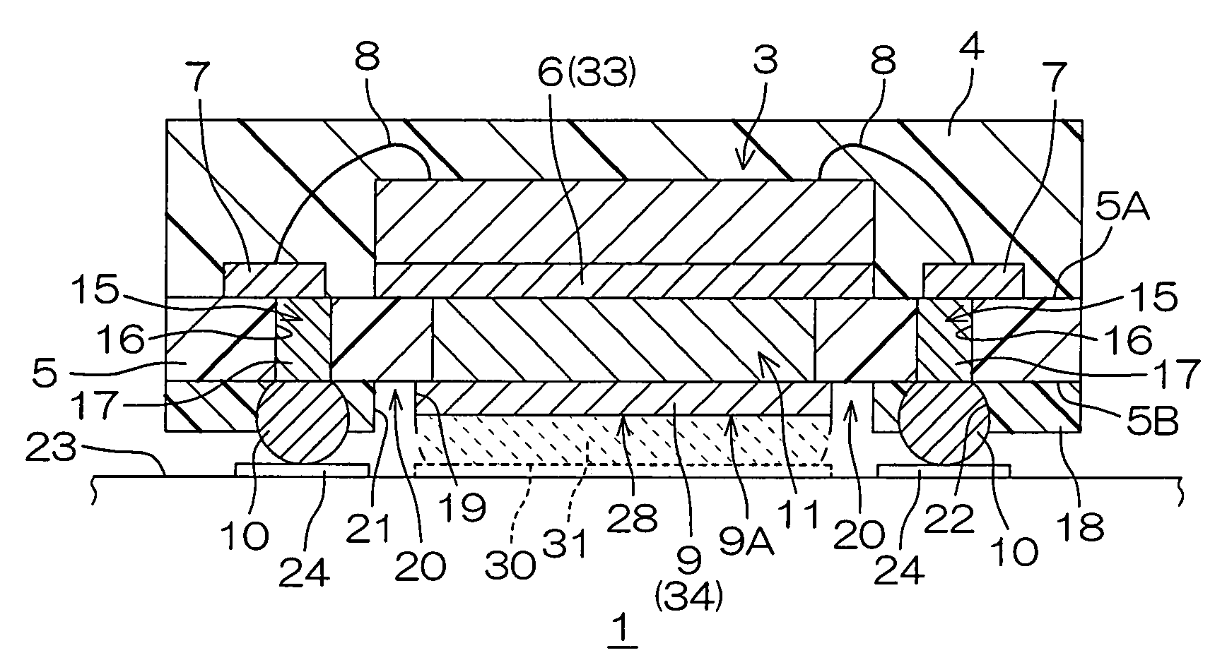
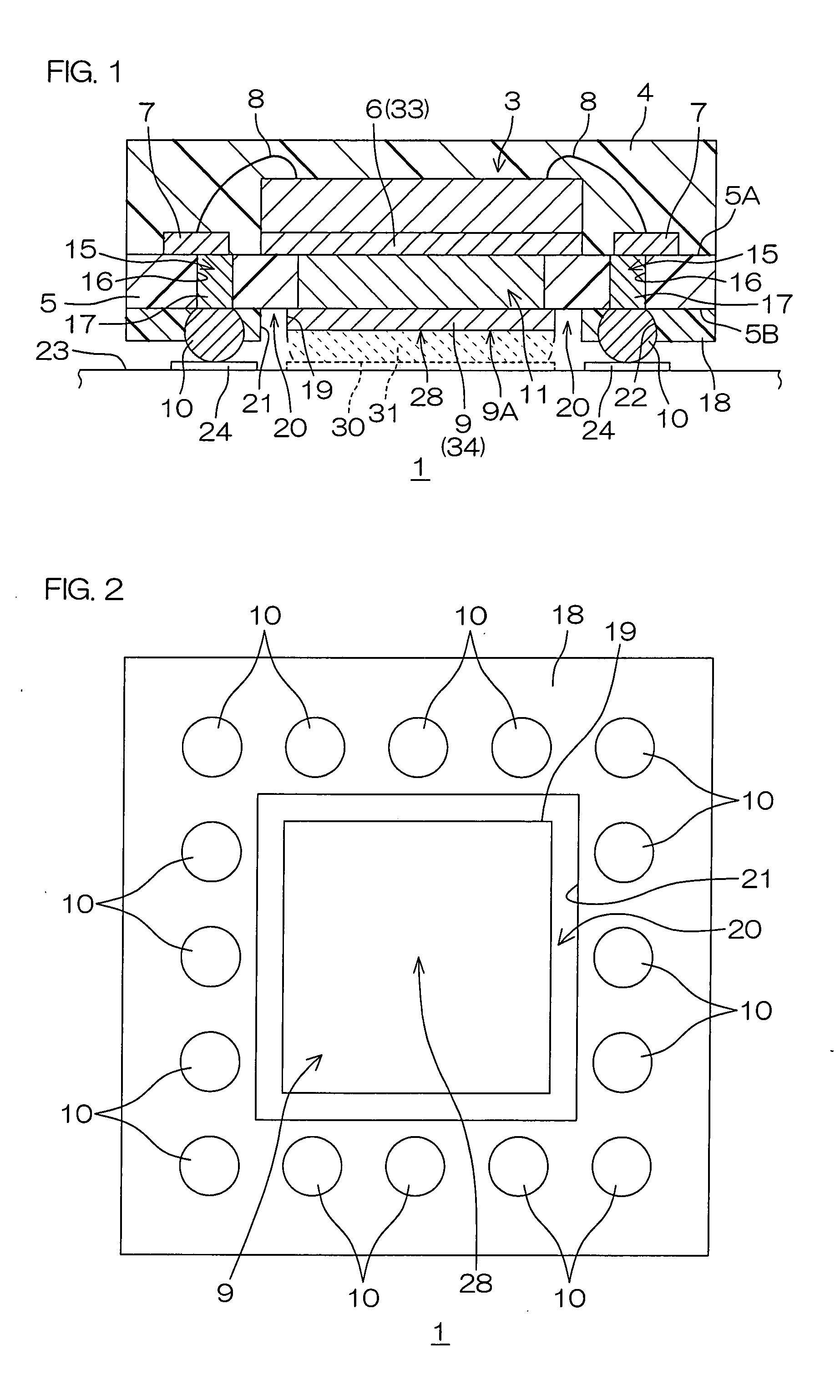
[0038]FIG. 1 is a schematic sectional view showing the construction of a semiconductor device according to one embodiment of the present invention. FIG. 2 is a schematic plan view illustrating a surface of the semiconductor device of FIG. 1 to be opposed to a mount board.

[0039]The semiconductor device 1 is a semiconductor device employing a BGA (Ball Grid Array) package, and includes an insulative substrate 5 of an insulative resin (e.g., a glass epoxy resin), a semiconductor chip 3 mounted on the insulative substrate 5, and a resin seal 4 which seals the semiconductor chip 3 and one surface 5A of the insulative substrate 5 opposed to the semiconductor chip 3.

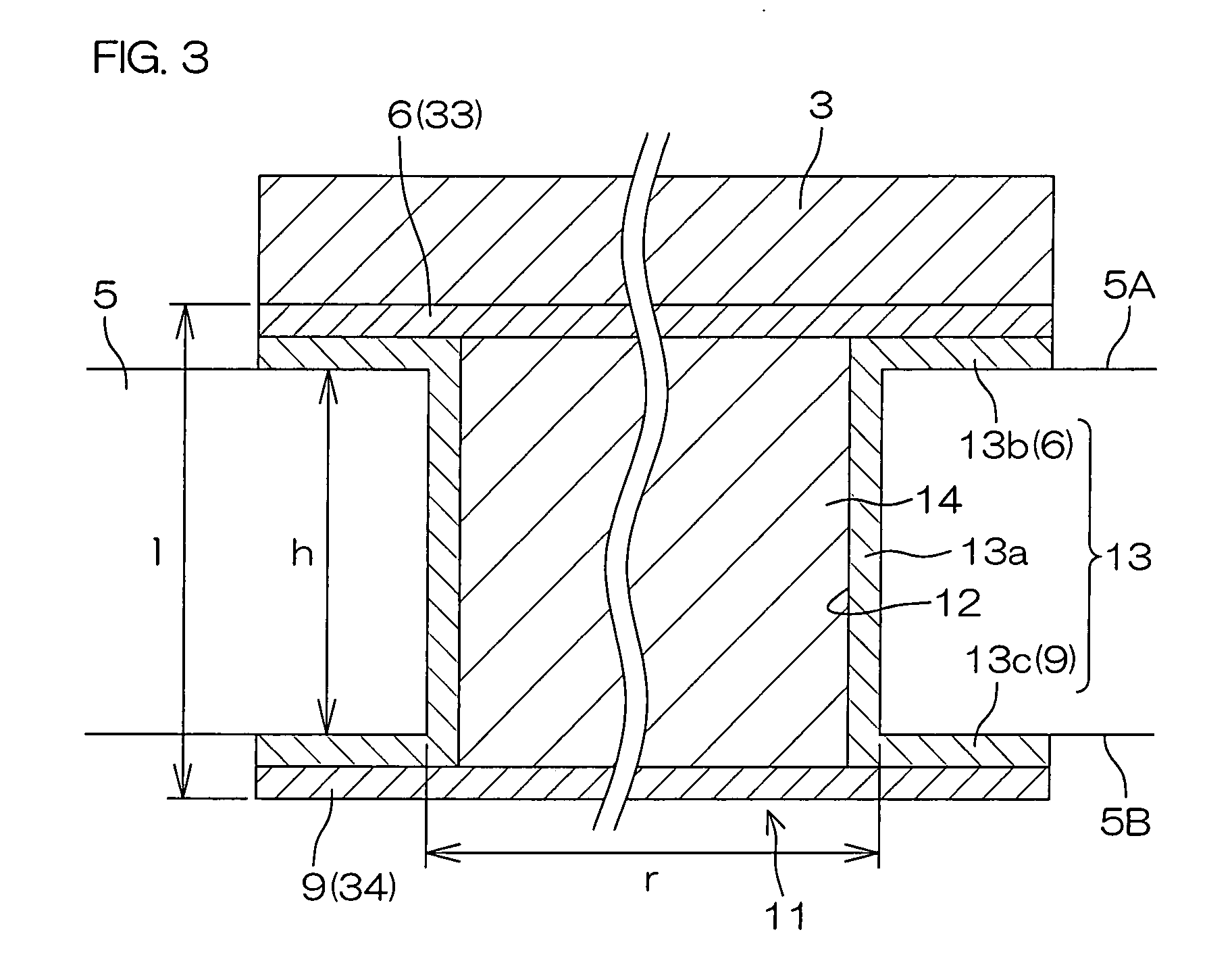
[0040]An island 6 and internal terminals 7 are provided on the one surface 5A of the insulative substrate 5.

[0041]The island 6 is composed of a metal material (e.g., copper or the like) having electrical co...


PUM


Abstract

A semiconductor device according to the present invention includes an island provided on one surface of a resin substrate, an external terminal provided on the other surface of the substrate, a thermal pad provided on the other surface of the substrate in opposed relation to the island, a heat conduction portion extending through the substrate from the one surface to the other surface to connect the island to the thermal pad in a thermally conductive manner, and a solder resist portion provided on the other surface of the substrate and having a heat dissipation opening which defines a gap with respect to an outer periphery of the thermal pad and a terminal opening which exposes the external terminal.

Description

BACKGROUND OF THE INVENTION[0001]1. Field of the Invention[0002]The present invention relates to a semiconductor device and, more specifically, to a BGA (Ball Grid Array) semiconductor device and an LGA (Land Grid Array) semiconductor device.[0003]2. Description of Related Art[0004]Surface-mountable packages which permit surface mounting of semiconductor devices on a wiring board are frequently used for increasing the integration density of the semiconductor devices on the wiring board. BGA packages are known as typical examples of such surface-mountable packages.[0005]A BGA semiconductor device employing a BGA package includes a substrate and a semiconductor chip mounted on the substrate. The substrate is, for example, an insulative substrate of a glass epoxy resin. Provided on one surface of the insulative substrate are an island on which a semiconductor chip is bonded, and internal terminals respectively electrically connected to pads on a surface of the semiconductor chip via bo...

Claims


Application Information

Patent Timeline
Patent Type & Authority Applications(United States)
IPC IPC(8): H01L23/36
CPCH01L23/3677H01L23/49816H01L2924/15311H01L2224/73265H01L2224/48091H01L2224/48227H01L2924/01078H01L2924/01079H01L2924/14H01L24/48H01L2224/45144H01L2924/00H01L2924/00014H01L24/45H01L2924/181H01L2224/32225H01L2924/00012H01L23/48
Inventor HAGA, MOTOHARUKASUYA, YASUMASA
Owner ROHM CO LTD
Why Eureka
Try Eureka