Unlock instant, AI-driven research and patent intelligence for your innovation.

Subminiature electronic device having hermetic cavity and method of manufacturing the same

a technology of electronic devices and hermetic cavities, which is applied in the direction of semiconductor devices, semiconductor device details, electrical devices, etc., can solve the problems of high material cost, inability to hermetically seal the gas, and high cost of flip chip fabrication, so as to achieve the effect of less cos

Inactive Publication Date: 2008-08-14
BESDON TECH CORP
View PDF2 Cites 14 Cited by
  • Summary
  • Abstract
  • Description
  • Claims
  • Application Information

AI Technical Summary

Benefits of technology

[0024]A scope of the present invention is to provide a subminiature electronic device with a sealed cavity and its manufacturing method at less cost. A large substrate having formed a plurality of identical microstructures is provided and a sacrificial layer comprising polymer is coated onto each of the microstructures. A protective layer containing glass powders is then applied to encapsulate the sacrificial layer. Afterwards, the sacrificial layer is removed so as to form a cavity between the microstructure and the protective layer. The whole protective layer is melted at elevated temperature to hermetically seal the cavity after cooling.
[0026]The protective layer is homogeneous material comprising glass that substitutes sealing material and lid, sealing material and cap, or sealing material and base plate of the described examples of conventional devices. From another viewpoint, the present invention extends the scope of sealing material to replace the function of cap, lid, or base plate. Therefore, the present invention is more concisely constructed so that the material cost is reduced and the manufacturing method becomes simplified too.
[0027]Another scope of the present invention is to provide a subminiature electronic device with a sealed cavity that is smaller in size. Because the protective layer comprising glass is directly disposed over the microstructures, precise assembly between lid and base, cap and substrate, or chip and base plate of conventional devices is no longer required. So, the dimension tolerance required for assembly is substantially reduced. Furthermore, the length and width of the packaged device can be made as small as those of the chip. Therefore, a chip scale packaged device is accomplished in a large substrate level. The present invention exhibits significant advantages over the conventional devices in the chip scale package because the costly flip chip assembly technique is not required anymore.

Problems solved by technology

Polymeric materials are widely used in the electronic industry such as epoxy, polyimide, and silicone, but they cannot hermetically seal the gas.
However, the fabricating cost by flip chip is very expensive because the dimension of chip 11 is extremely small and fine.
But, the material cost is high, particularly the gold-containing material such as sealing material, lid, bonding wires, and bonding conductors.
Also, the fabricating cost is high because of the low productivity that the lid and base, or the cap and substrate must be precisely assembled one by one.
The fabricating cost is particularly high for a chip scale package by the flip chip technique, wherein the chip is bonded to base plate one by one too.
As the device becomes smaller, the conventional assembly technique becomes very challenging to result in much higher fabricating cost.
However, bonding two large substrates is very difficult because of thermal mismatch of the two large substrates after melting the sealing material at high temperature unless the material, thickness, and geometry of the two large substrates are exactly the same.
Besides, the large substrate containing caps, bases, and base plates is usually made of ceramic material fired at a temperature more than 1000° C. so that the dimensions can not be precisely controlled.
The larger the substrate, the more serious the problem will be.

Method used


Image

  • Subminiature electronic device having hermetic cavity and method of manufacturing the same
  • Subminiature electronic device having hermetic cavity and method of manufacturing the same
  • Subminiature electronic device having hermetic cavity and method of manufacturing the same

Examples


Embodiment Construction

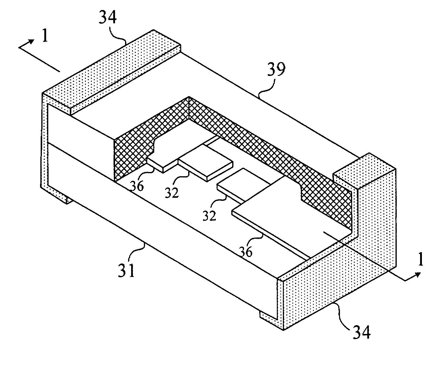
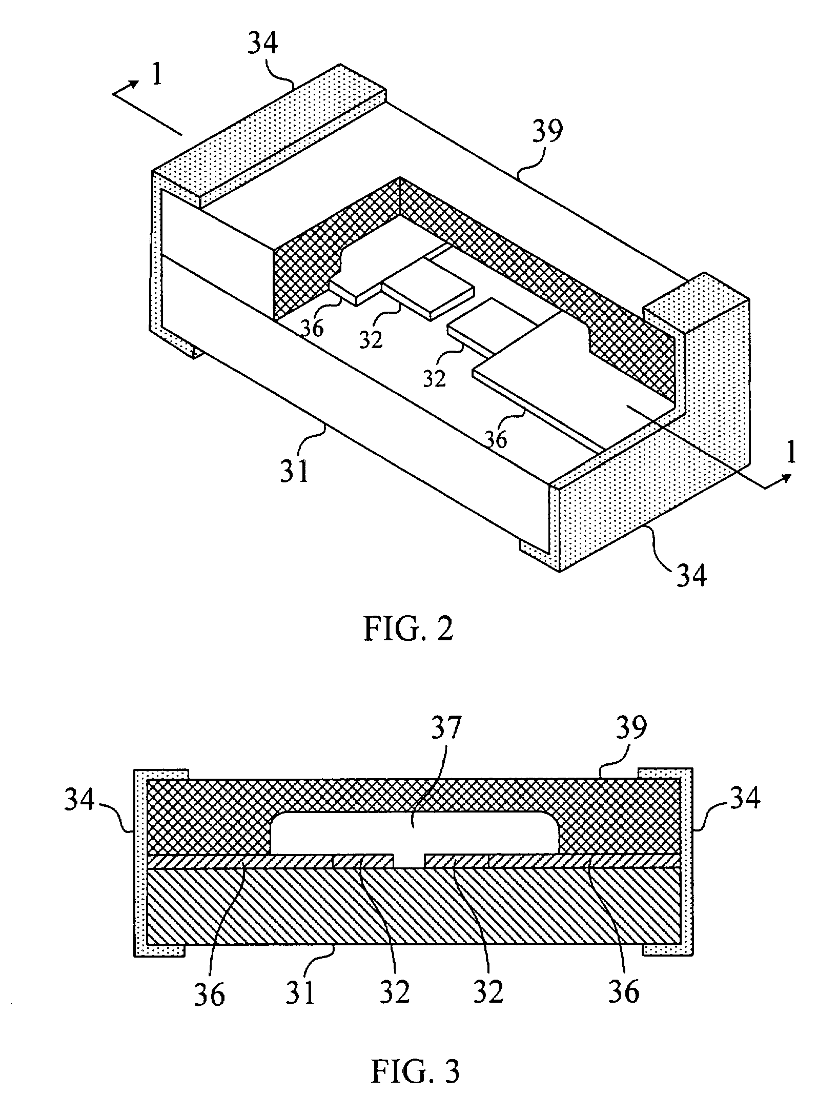
[0045]FIG. 2 and FIG. 3 illustrate a preferred embodiment of the present invention with two terminals. The device can be a chip-type over-voltage protector by gas discharge techniques. FIG. 2 is a perspective view wherein protective layer 39 is partially removed to reveal the internal structure. FIG. 3 is a cross-sectional view of FIG. 2 along the centerline of width (1-1 line). The device comprises a substrate 31, a protective layer 39, a cavity 37, two discharge electrodes 32, two termination pads 36, and two terminals 34.

[0046]The substrate 31 is electrically insulating and is made of alumina of more than 90% purity, glass, or other ceramics. Alumina of 96% purity is widely used with a thickness of 0.2 to 1.0 mm.

[0047]The microstructure includes two discharge electrodes 32 disposed on the top surface of substrate 31 and separated by a tiny gap, wherein one of the discharge electrodes connects with the circuits to be protected while the other one connects with the ground. Over-vol...


PUM


Abstract

The invention discloses a subminiature electronic device with a hermetic cavity and method of manufacturing the same. It particularly relates to a chip type or chip scale packaged electronic device produced in substrate level. Firstly, a sacrificial layer is coated onto each of the identical microstructures disposed on a large substrate. A protective layer containing glass powders is then applied to encapsulate the sacrificial layer. Afterwards, the sacrificial layer is removed so as to form a cavity between the microstructure and the protective layer. The whole protective layer is then melted at elevated temperature to seal the cavity in an environment of specific gas. Finally, the large substrate is diced into a plurality of individual devices with a hermetic cavity over the microstructure. The applicable fields include micro-electronic circuits, micro-vibration systems, micro electrical-mechanical systems (MEMS), and gas discharge apparatuses.

Description

BACKGROUND OF THE INVENTION[0001]1. Field of the Invention[0002]The invention relates to a subminiature electronic device that is mounted directly onto the surface of circuit boards. The invention generally relates to the package of a subminiature device having a sealed cavity over microstructure that is disposed on a substrate. Further, the cavity can be hermetically sealed to enclose a specific gas inside. More particularly, the invention discloses a chip scale packaged device having a hermetic cavity that is fabricated in the substrate level at inexpensive cost.[0003]2. Description of the Prior Art[0004]A hermetic cavity plays an important role in electronic devices by providing a sealed free space over microstructure and enclosing a specific gas inside. Therefore, the microstructure can be operated in a safe and stable environment because air and other gases in the surrounding atmosphere are isolated from the cavity.[0005]The application of hermetic cavities can be roughly class...

Claims


Application Information

Patent Timeline
IPC IPC(8): H01L23/20H01L21/54
CPCH01L23/3121H01L23/315H01L2924/1461H01L24/48H01L2924/09701H01L2924/04941H01L2924/01079H01L2924/01078H01L2924/01029H01L2224/32225H01L2224/48091H01L2224/48227H01L2224/73265H01L2924/00014H01L2924/00H01L2224/451H01L2224/45015H01L2224/45124H01L2924/14H01L2924/16195H01L2224/45144H01L24/45H01L2924/20752H01L2924/20753H01L2924/20755H01L2924/00015H01L2924/20754H01L2924/2075
Inventor TSAI, CHON-MING
Owner BESDON TECH CORP