Semiconductor package having impedance matching device

a technology of impedance matching and semiconductors, applied in the direction of coupling devices, waveguide type devices, printed circuit aspects, etc., can solve the problems of reduced increased cost and reduction of available space on the substrate, and reduced wiring area of matching networks. achieve the effect of impedance matching, enhance flexibility and interchangeability in wiring layout, and effectively reduce wiring area

Active Publication Date: 2008-08-14
ADVANCED SEMICON ENG INC
View PDF14 Cites 14 Cited by
  • Summary
  • Abstract
  • Description
  • Claims
  • Application Information

AI Technical Summary

Benefits of technology

[0011]The semiconductor package constructed according to the present invention comprises an impedance matching device to effectively achieve impedance matching between different systems integrated in the semiconductor package. The impedance matching device also helps to effectively reduce the wiring area of an impedance matching network of the semiconductor package and enhance the flexibility and interchangeability in layout of the wiring.

Problems solved by technology

However, this method results in increased cost and reduction of available space on the substrate.
Further, the wiring area of the matching network is reduced, and flexibility and interchangeability in layout of the wiring is limited.

Method used


Image

  • Semiconductor package having impedance matching device
  • Semiconductor package having impedance matching device
  • Semiconductor package having impedance matching device

Examples


first embodiment

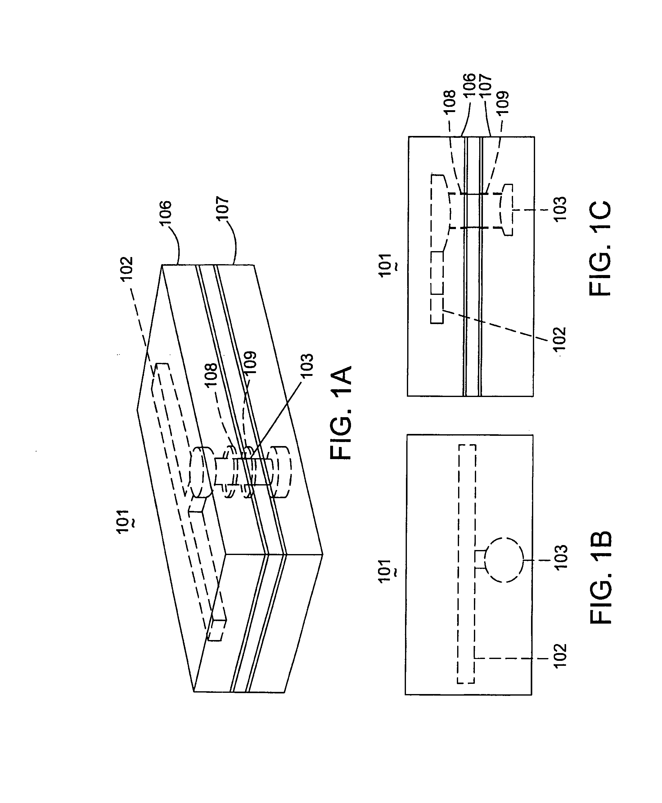
[0016]Referring to FIGS. 1A to 1C, a substrate 101 of a semiconductor package having an impedance matching device according to the present invention is schematically shown. The substrate 101, in an exemplary form of a system in package, has a multilayer substrate including a first substrate unit 106 and a second substrate unit 107 stacked over each other using conventional laminating technology. In the drawings of all embodiments of the present invention, the first and second substrate units 106 and 107 are shown, in an exaggerated manner, to be separated from each other for clear illustration purpose. The substrate 101 as shown is also only a portion of the whole semiconductor package in order to clearly show the impedance matching device thereof. The remaining portion of the whole semiconductor package is not shown for simplicity and clarity purposes for it forms no novel part of the present invention. Thus, a detailed description hereinafter is given to the impedance matching dev...

second embodiment

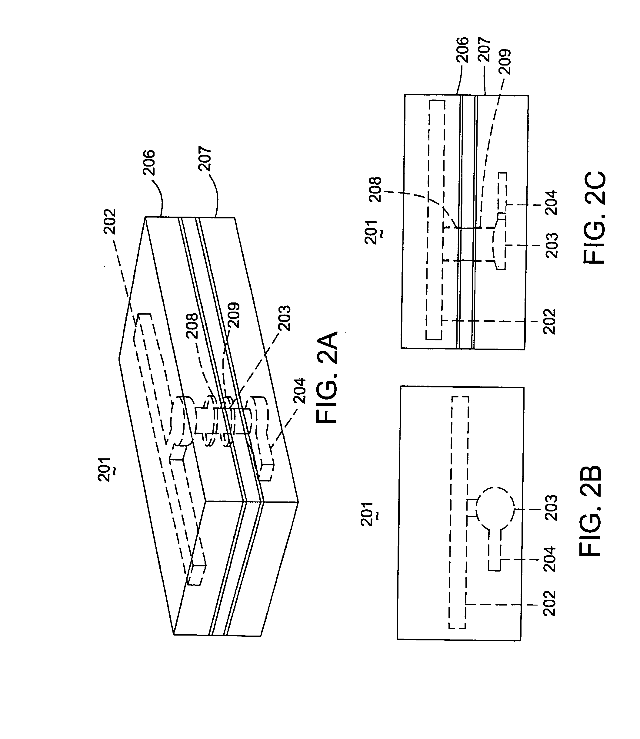
[0020]Reference is now directed to FIGS. 2A to 2C, which schematically represent a substrate 201 having an impedance matching device according to the present invention. In this embodiment, a vertical conductive line and a stub transmission line are employed for impedance matching. As shown in FIG. 2A, the substrate 201 has a substrate including a first substrate unit 206 and a second substrate unit 207, and a metal wiring 202 provided in at least one insulation layer (unlabeled) of the first substrate unit 206 (or provided on a surface of at least one insulation layer of the first substrate unit 206), and above the second substrate unit 207. The metal wiring 202 extends in a horizontal direction for transmitting an electrical signal and electrically connects the first and second substrate units 206, 207 with a semiconductor chip (not shown) of the substrate 201.

[0021]To match the impedance of the metal wiring 202 with that of the semiconductor chip, a vertical conductive line 203 an...

third embodiment

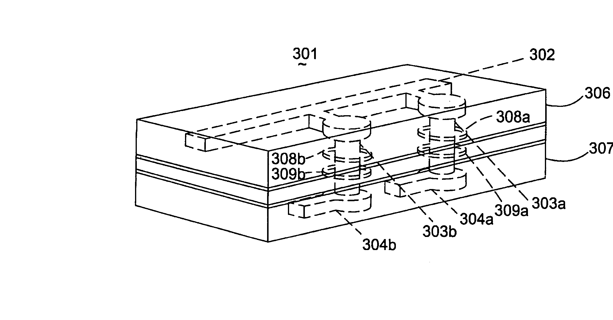
[0024]Reference is now directed to FIGS. 3A to 3C, which schematically represent a substrate 301 having an impedance matching device according to the present invention. In this embodiment, a plurality of vertical conductive lines (two shown) and a plurality of stub transmission lines (two shown) are employed for impedance matching. As shown in FIG. 3A, the substrate 301 has a substrate including a first substrate unit 306 and a second substrate unit 307, and a metal wiring 302 provided in at least one insulation layer (unlabeled) of the first substrate unit 306 (or provided on a surface of at least one insulation layer of the first substrate unit 306), and above the second substrate unit 307. The metal wiring 302 extends in a horizontal direction for transmitting an electrical signal and electrically connects the first and second substrate units 306, 307 with a plurality of semiconductor chips (not shown) of the substrate 301.

[0025]To match the impedance of the metal wiring 302 with...


PUM


Abstract

A semiconductor package having an impedance matching device is disclosed, which is especially applicable to conventional system-in-package structures and system packaging design with high-density I / O design. The impedance matching device achieves impedance matching between a semiconductor chip and a signal transmission wiring on the substrate or between different systems integrated in the semiconductor package by employment of a vertical conductive line or combination of a vertical conductive line and a stub transmission line. The vertical conductive line is electrically connected with the signal transmission wiring on the substrate at one end thereof, and the stub transmission line may be further connected to the other end of the vertical conductive line. This impedance matching device helps to effectively reduce the wiring area of an impedance matching network of the semiconductor package and enhance the flexibility and interchangeability in layout of the wiring.

Description

BACKGROUND OF THE INVENTION[0001]1. Field of the Invention[0002]The present invention relates to a semiconductor package, and particularly to a semiconductor package having an impedance matching device for achieving impedance matching between different systems integrated in the semiconductor package by means of a vertical conductive line or combination of a vertical conductive line and a stub transmission line.[0003]2. Description of Prior Art[0004]In the current electronic industry, electronic products, such as mobile phones, bluetooth systems, personal digital assistances and digital cameras, are increasingly required to be lightweight, thin, compact and multifunctional. Consequently, both electronic components and wiring in these electronic products have been increasing in number and reducing in size. This necessitates the introduction of system packaging technology so that subsystems, for example, microprocessors and memory units can be integrated in a semiconductor chip to obta...

Claims


Application Information

Patent Timeline
Patent Type & Authority Applications(United States)
IPC IPC(8): H01L23/52
CPCH01L25/16H01L2223/6616H01L2223/6627H01L2924/1903H01P5/02H05K1/025H01L2924/0002H05K2201/096H05K2201/09781H01L2924/00
Inventor CHUANG, TSENG-YINGLI, PAO-NAN
Owner ADVANCED SEMICON ENG INC
Why Eureka
Try Eureka