
High pass filter circuit with low corner frequency

a filter circuit and corner frequency technology, applied in the field of high pass filter circuits, can solve the problems of significant cost increase, and achieve the effect of accurate bias voltage and low cos

Inactive Publication Date: 2008-08-14
MEDIATEK INC
View PDF10 Cites 1 Cited by
  • Summary
  • Abstract
  • Description
  • Claims
  • Application Information

AI Technical Summary

Benefits of technology

[0004]To solve the foregoing drawbacks in the prior art, it is an objective of the present invention to provide a high pass filter circuit having a low corner frequency and providing accurate bias voltage with low cost

Problems solved by technology

The resistor with large impedance occupies a large area in integrated circuits now, which significantly increases the cost.

Method used


Image

  • High pass filter circuit with low corner frequency
  • High pass filter circuit with low corner frequency
  • High pass filter circuit with low corner frequency

Examples


Embodiment Construction

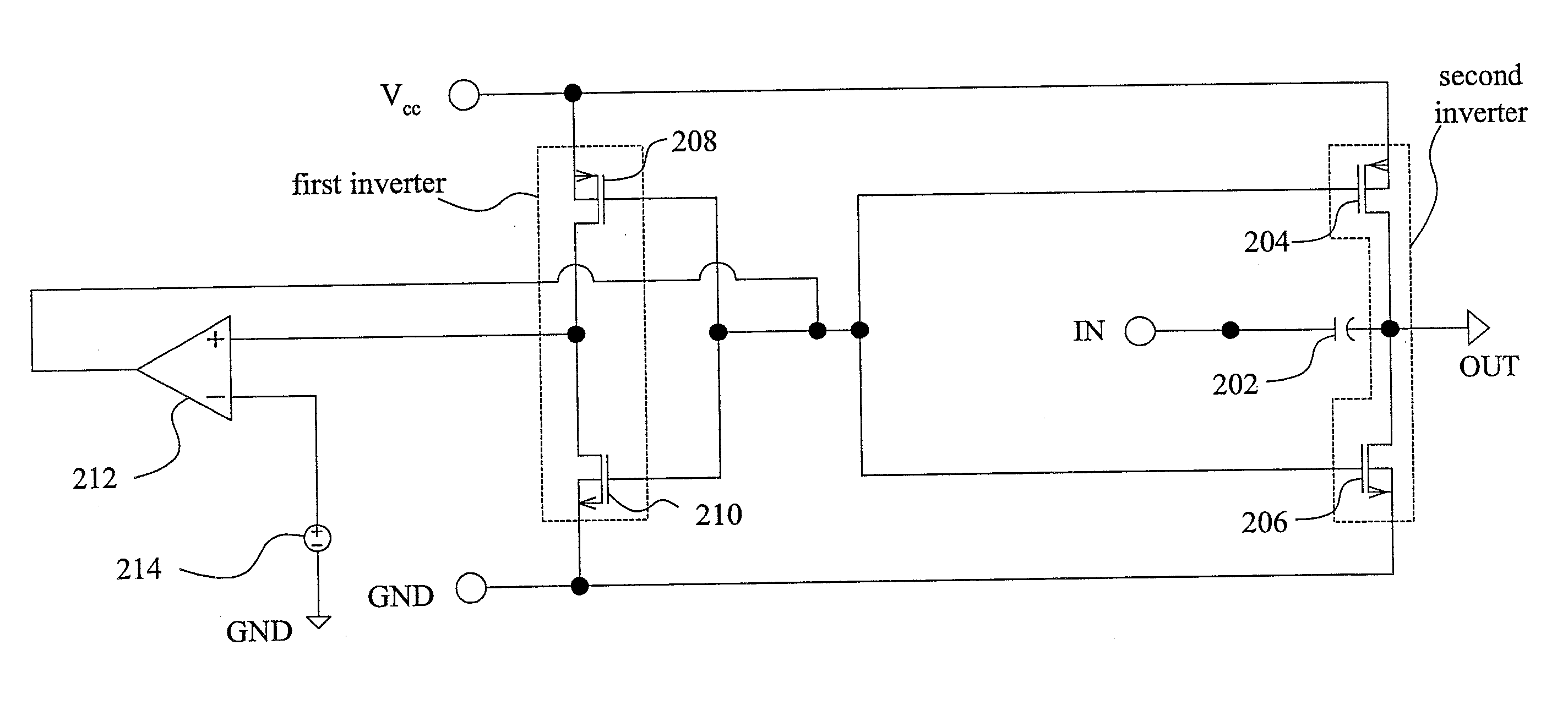
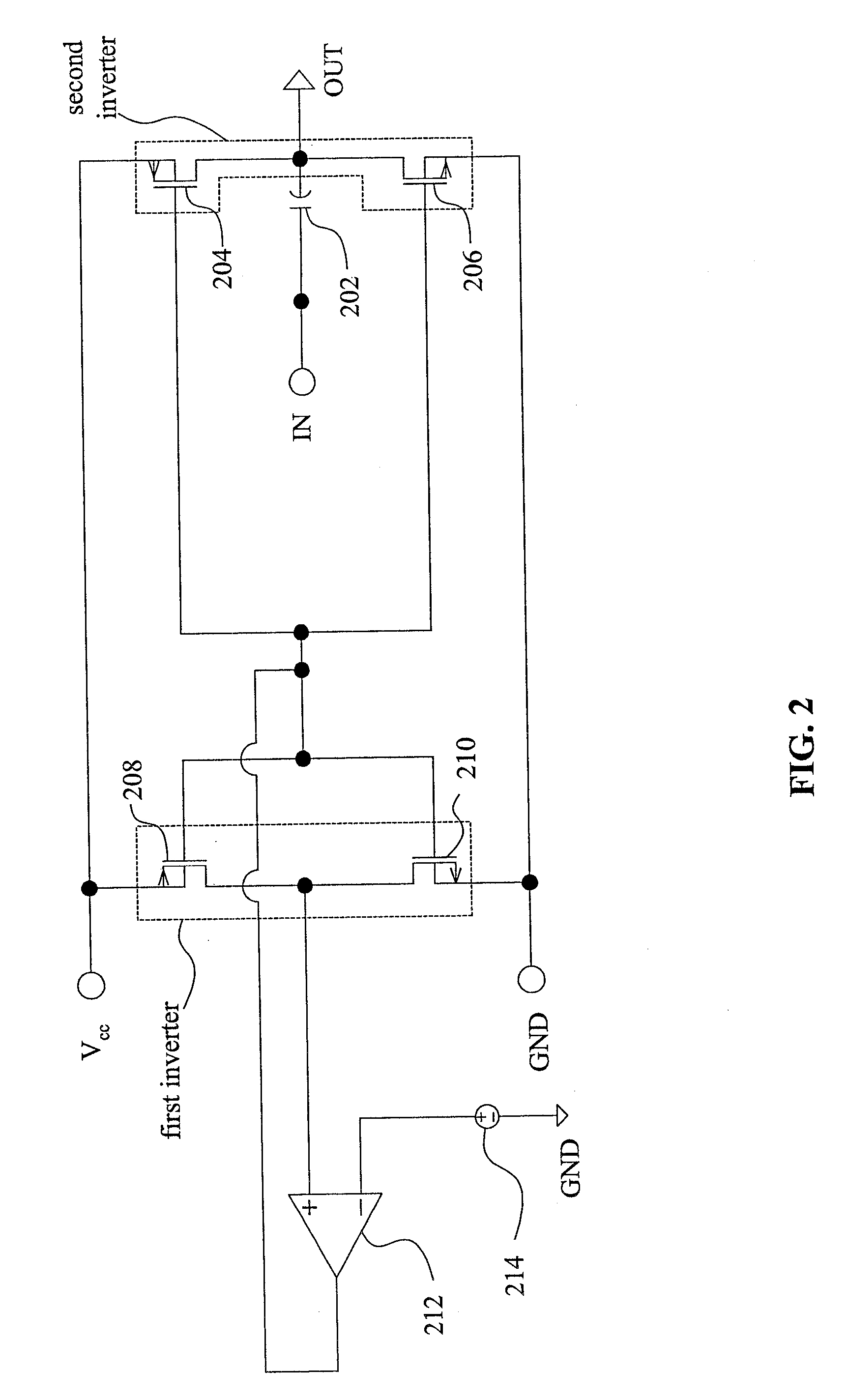
[0011]Please refer to FIG. 2, which shows a high pass filter circuit according to a preferred embodiment of the present invention. The high pass filter circuit has a signal input terminal IN and a signal output terminal OUT. In addition, the high pass filter circuit includes a capacitor 202, a first inverter composed of transistors 208, 210, a second inverter composed of transistors 204, 206, a voltage source 214, and an operational amplifier 212. For the DC offset removal, the capacitor 202 is arranged to connect with the second inverter providing a large impedance to apply an AC-coupling to block the DC offset. The transistors in the first and second inverters are CMOS transistors in this preferred embodiment. In this embodiment, the transistors 204, 208 are p-MOS transistors, the transistors 206, 210 are n-MOS transistors. The capacitor 202 is coupled between the signal input terminal IN and the signal output terminal OUT. The drain of the transistor 204 and the drain of the tran...


PUM


Abstract

A high pass filter circuit having a signal input terminal and a signal output terminal. The high pass filter circuit is provided with a voltage source, first and second inverters, and a capacitor. The voltage source provides a DC bias voltage. The first inverter couples to the voltage source to invert the DC bias voltage. The second inverter couples to the first inverter and a signal output terminal respectively. The second inverter inverts the DC bias voltage inverted by the first inverter to provide the DC bias voltage to the signal output terminal. The second inverter also provides large impedance at the signal output terminal. The capacitor is coupled between the signal input terminal and the signal output terminal to provide a low corner frequency in cooperation with the second inverter. The circuit further comprises an operational amplifier. The voltage source provides the DC bias voltage through the operational amplifier to avoid the total impedance at the output terminal that is decreased by the voltage source.

Description

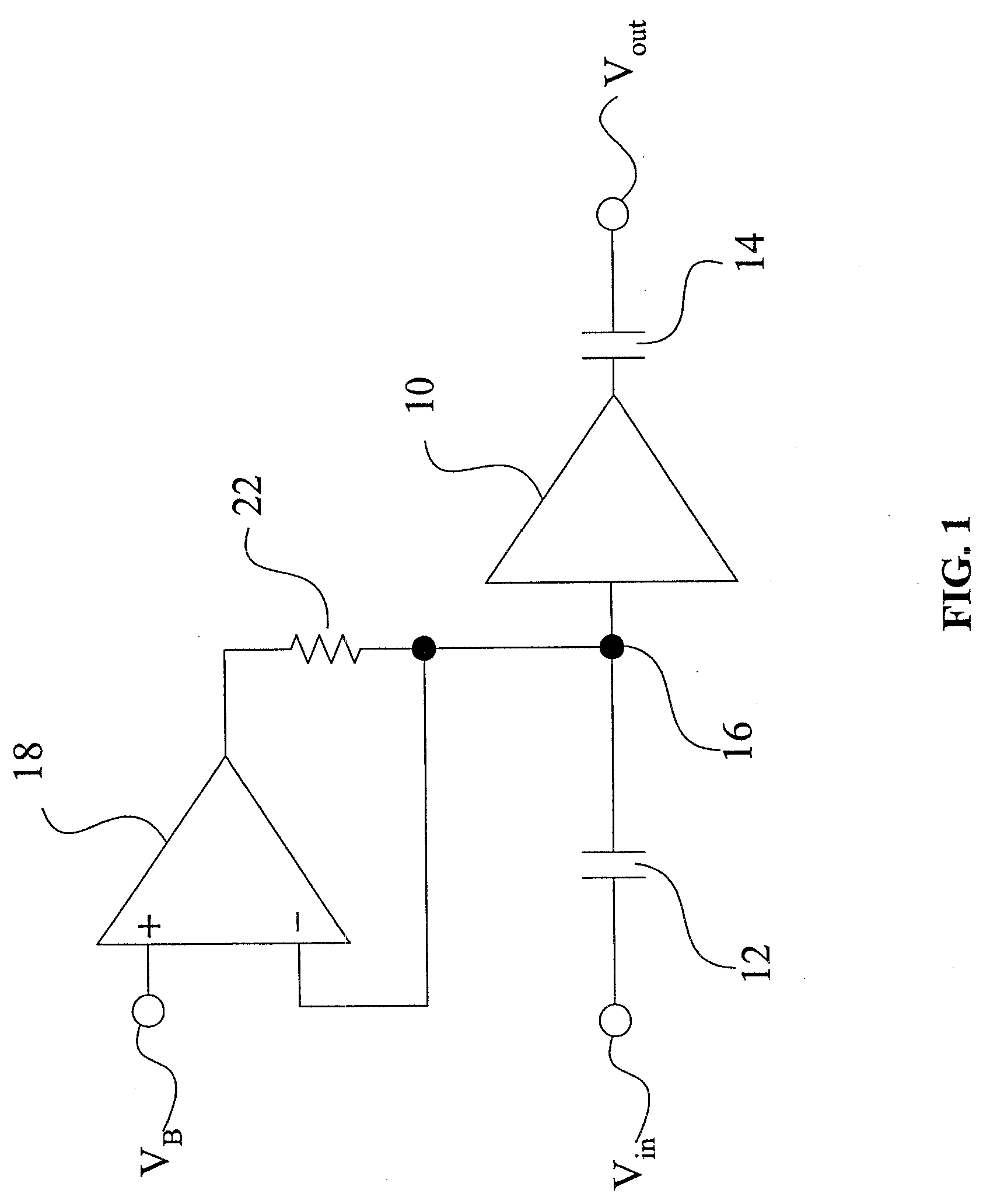
FIELD OF THE INVENTION[0001]The present invention generally relates to a high pass filter circuit, more particularly, to a high pass filter circuit having a low corner frequency and providing accurate biasing voltage.BACKGROUND OF THE INVENTION[0002]Direct conversion technique is going to be employed widely nowadays in radio frequency (RF) applications. The influence of the DC offset cancellation is a significant topic for a direct conversion receiver (DCR). For example, an AC-coupled circuit is typically used to implement DC offset cancellation to filter out the DC subsequently. In addition, it is necessary to provide a DC bias voltage at this stage to the following module, such as an analog-to-digital converter (ADC).[0003]A typical prior art for voltage biasing scheme is shown in FIG. 1. As disclosed in U.S. Pat. No. 5,760,651, an inductorless voltage biasing circuit is disclosed. An amplifier 10 is coupled with capacitors Cin 12 and Cout 14 between input and output terminals Vin...

Claims


Application Information

Patent Timeline
Patent Type & Authority Applications(United States)
IPC IPC(8): H03B1/00H04B1/10
CPCH03H11/04
Inventor CHIU, CHINQ-SHIUNCUI, JIQING
Owner MEDIATEK INC
Learn More