Inertial sensor and manufacturing method of the same

a technology of inertial sensor and manufacturing method, which is applied in the direction of acceleration measurement using interia forces, acceleration measurement in multiple dimensions, instruments, etc., can solve the problems of reducing the strength of the beam, affecting the accuracy and unable to achieve the strength (reliability) of the structure body and the sensitivity of the inertial sensor. achieve the effect of wide acceleration range and wide dynamic rang

Inactive Publication Date: 2008-08-21
HITACHI LTD
View PDF8 Cites 21 Cited by
  • Summary
  • Abstract
  • Description
  • Claims
  • Application Information

AI Technical Summary

Benefits of technology

[0011]The first object of the present invention is to provide an inertial (acceleration) sensor by the MEMS, which can achieve both a strength (reliability) of a structure body and a sensitivity

Problems solved by technology

A problem to be solved by the present invention is that, first, it becomes hard to achieve both a strength (reliability) of the structure body and a sensitivity of the inertial sensor when the inertial sensor by the MEMS of the prior art is miniaturized.
However, in this case, if the inertial sensor itself is miniaturized or thinned, the strength of the beam is significantly lowered.
In other words, since it is necessary to weaken the strength of the beam supporting the weight for improving the sensitivity of the inertial sensor, it becomes hard to simultaneously secure the strength and the sensitivity of the inertial sensor.
However, it is hard to secure the dynamic range in the prior art.
In other words, if the spring constant is made smaller for achieving the high sensitivity with respect to the small acceleration, the weight is significantly displaced when the large

Method used


Image

  • Inertial sensor and manufacturing method of the same
  • Inertial sensor and manufacturing method of the same
  • Inertial sensor and manufacturing method of the same

Examples


first embodiment

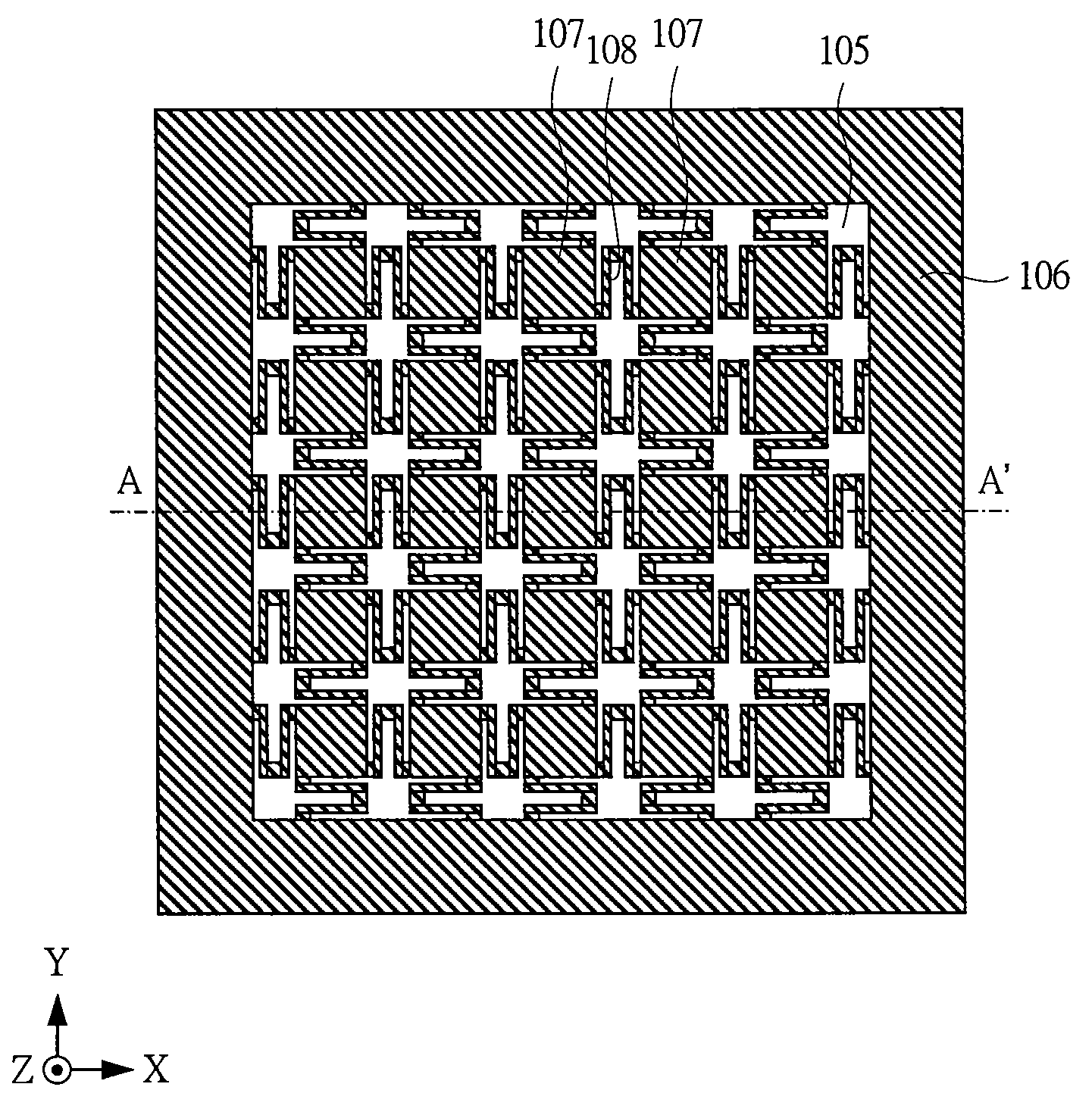
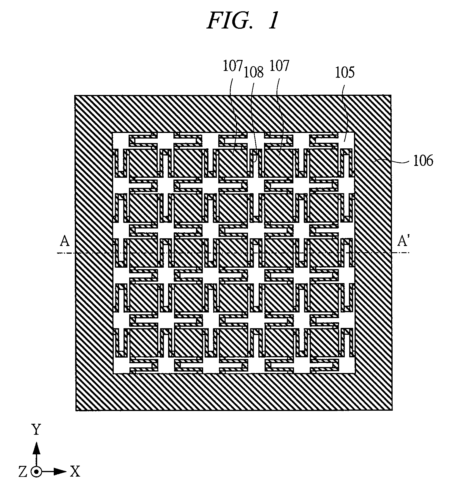
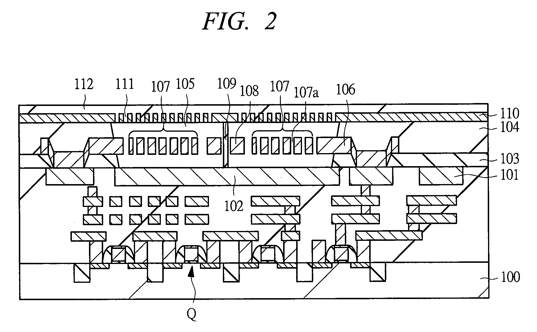
[0067]An inertial sensor according to the first embodiment will be described with reference to the accompanying drawings. FIG. 1 is a plan view showing a mechanism portion (main portion) of an inertial sensor according to the first embodiment. As shown in FIG. 1, a frame 106 formed by a thin film is formed in the periphery. The frame 106 is fixed to a semiconductor substrate in which the inertial sensor is formed. A cavity portion 105 is formed inside the frame 106, and a plurality of divided weights 107 are arranged inside the cavity portion 105 via a plurality of beams (elastic bodies) 108. In other words, a plurality of divided weights 107 are arranged inside the cavity portion 105 in a two-dimensional manner (in a direction of an X axis and a direction of a Y axis), and the divided weights 107 are connected to each other by an elastically deformable beams 108. The plurality of divided weights 107 formed in the above-mentioned manner are designed to be displaced in a direction of...

second embodiment

[0118]A one-axis acceleration (or vibration) sensor (inertial sensor) according to a second embodiment of the present invention will be described with reference to the accompanying drawings. FIG. 16 is a diagram schematically showing a planar layout of a movable structure body (sensor first layer) of the one-axis acceleration (or vibration) sensor in the second embodiment. FIG. 17 is a schematic cross sectional view for explaining an operation of the one-axis acceleration sensor in the second embodiment. The one-axis acceleration sensor in the second embodiment is also manufactured by the same manufacturing process as the first embodiment mentioned above.

[0119]A divided weights 202 formed in the sensor first layer are formed to have four trapezoidal shapes as shown in FIG. 16. The divided weight 202 is formed inside a cavity portion 201, and the divided weights 202 are connected to each other by beams 203. Each of the divided weights 202 is fixed to a frame 200 of the cavity portion...

third embodiment

[0128]The present invention can be applied also to a sensor which detects an acceleration in a direction parallel to a main surface of the semiconductor substrate. In the third embodiment, an example in which the present invention is applied to an acceleration sensor (inertial sensor) which detects an acceleration in a direction of an X axis will be described with reference to FIG. 21 and FIG. 22.

[0129]FIG. 21 is a schematic diagram showing a planar layout of a movable structure body in a one-axis acceleration sensor according to the third embodiment. FIG. 21 is a schematic diagram for explaining an operation of the one-axis acceleration sensor according to the third embodiment. The weights formed by a sensor first layer include five divided weights 301 to 305 arranged in the direction of the X axis as shown in FIG. 21. The divided weights 301 to 305 are connected to each other by beams, and the divided weight 301 and the divided weight 305 in both ends are fixed to a frame 300 surr...


PUM

PropertyMeasurementUnit
Weightaaaaaaaaaa
Massaaaaaaaaaa
Sensitivityaaaaaaaaaa

Abstract

A weight of an inertial sensor if formed from a plurality of divided weights, and the divided weights are connected to each other by elastically deformable beams. A movable range and a mass of each of the divided weights and a rigidity of each of the beams are adjusted and a plurality of deformation modes having different sensitivity ranges with respect to the acceleration are used in combination. By this means, it is possible to improve a detecting sensitivity of an acceleration and widen an acceleration response range.

Description

CROSS-REFERENCE TO RELATED APPLICATION[0001]The present application claims priority from Japanese Patent Application No. JP2006-181056 filed on Jun. 30, 2006, the content of which is hereby incorporated by reference into this application.TECHNICAL FIELD OF THE INVENTION[0002]The present invention relates to an inertial sensor by micro electro mechanical systems (MEMS) and a manufacturing technology of the same. More particularly, it relates to an integrated device of a semiconductor integrated circuit device and an inertial sensor and a manufacturing technology of the same.BACKGROUND OF THE INVENTION[0003]There has been developed a micro electro mechanical systems (MEMS) technology for forming a mechanical sensor such as a pressure sensor or an acceleration sensor, a miniaturized mechanical part such as a minute switch or a transducer, and a mechanical system, by using a micro-fabrication technology for forming a semiconductor integrated circuit device. The MEMS is broadly classifie...

Claims


Application Information

Patent Timeline
IPC IPC(8): G01P15/00G01P15/125H01R43/00H01B13/00
CPCG01P15/08G01P15/125Y10T29/49117G01P2015/0814G01P15/18G01P2015/0828G01P2015/084
Inventor FUKUDA, HIROSHIHANAOKA, YUKOFUJIMORI, TSUKASA
Owner HITACHI LTD
Why Eureka
Try Eureka