Programmable Resistive Memory Cell with Self-Forming Gap

a resistive memory cell and self-forming technology, applied in the direction of bulk negative resistance effect devices, semiconductor devices, electrical devices, etc., can solve the problems of slowing down one of the problems associated with the small dimensions of phase change cells, and affecting the heating effect of curren

Active Publication Date: 2008-08-21
MACRONIX INT CO LTD
View PDF99 Cites 40 Cited by
  • Summary
  • Abstract
  • Description
  • Claims
  • Application Information

AI Technical Summary

Problems solved by technology

Problems have arisen in manufacturing such devices with very small dimensions, and with variations in process that meet tight specifications needed for large-scale memory devices.
One problem associated with the small dimensions of phase change cells has arisen because of the thermal conductivity of materials surrounding the active region.
However, heat generated by the current through the materi...

Method used


Image

  • Programmable Resistive Memory Cell with Self-Forming Gap
  • Programmable Resistive Memory Cell with Self-Forming Gap
  • Programmable Resistive Memory Cell with Self-Forming Gap

Examples


Embodiment Construction

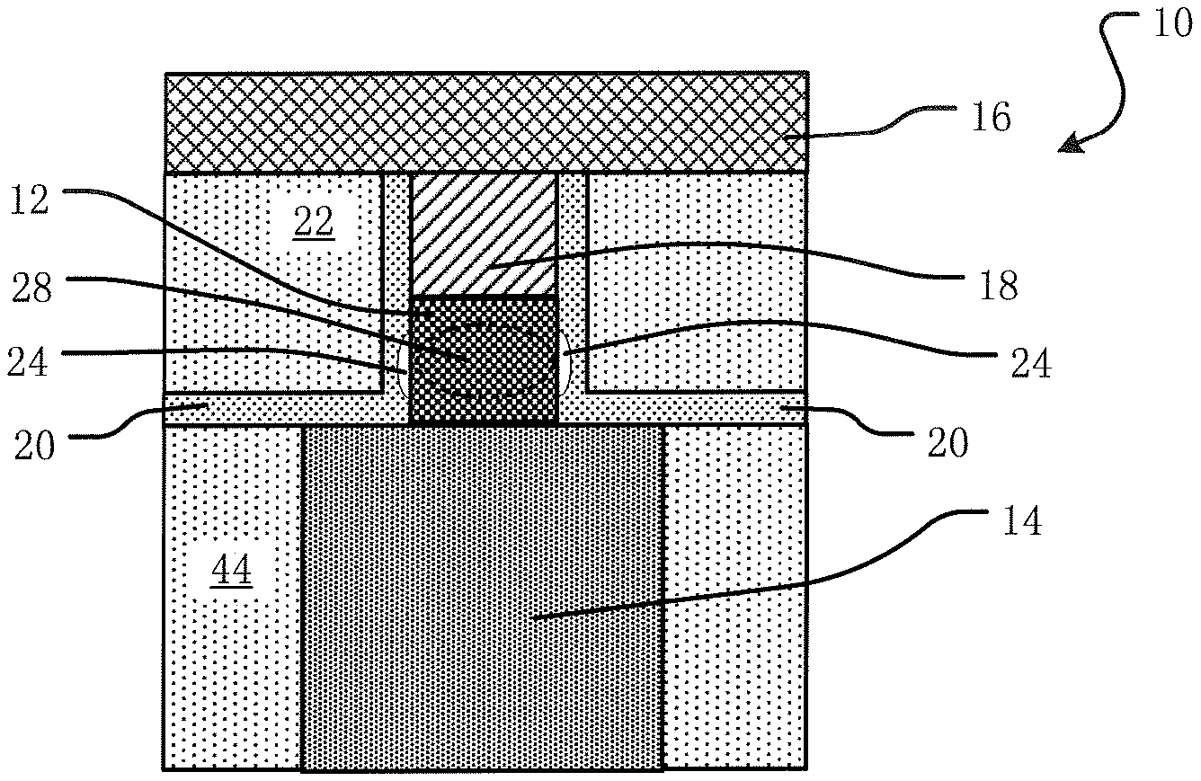
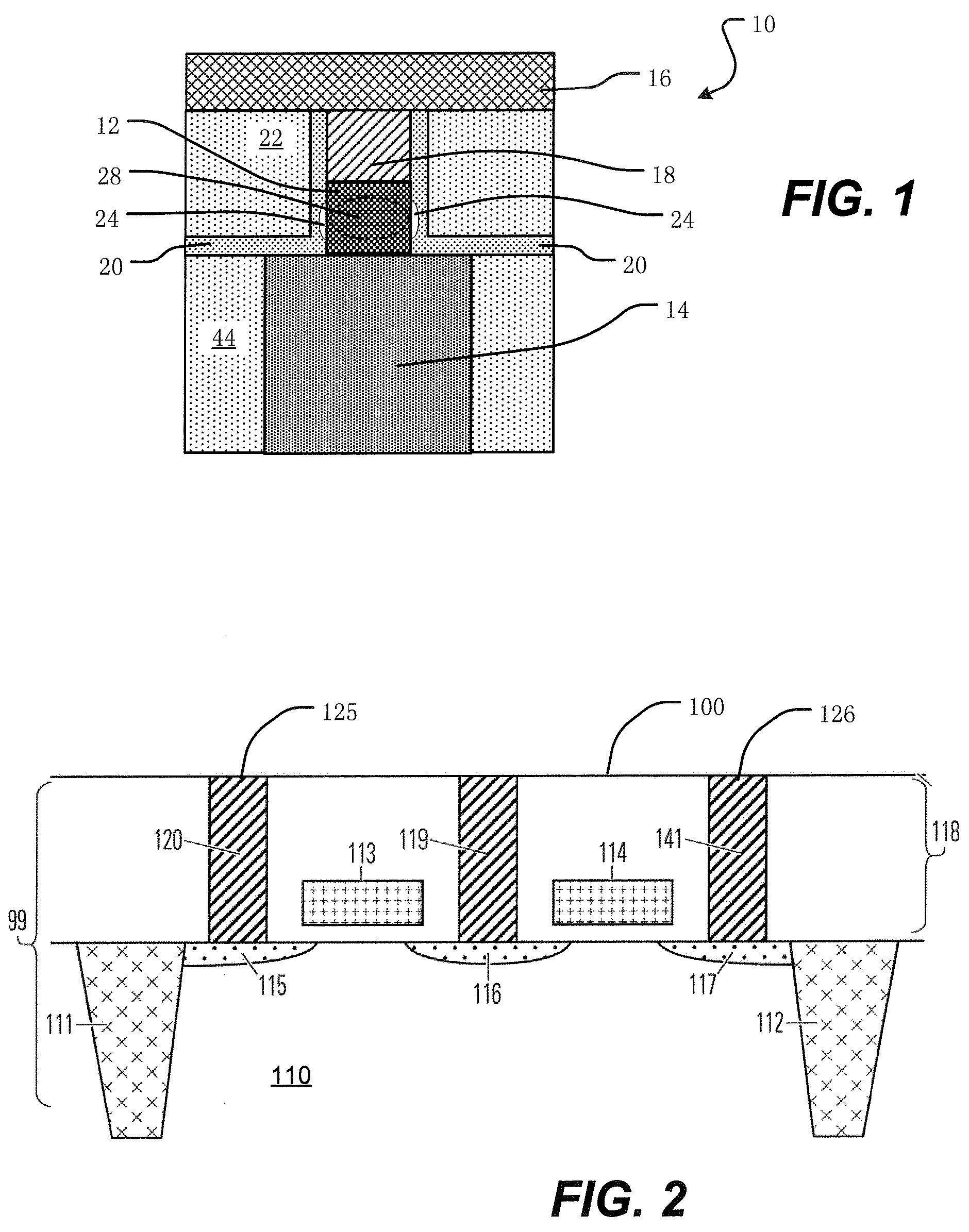
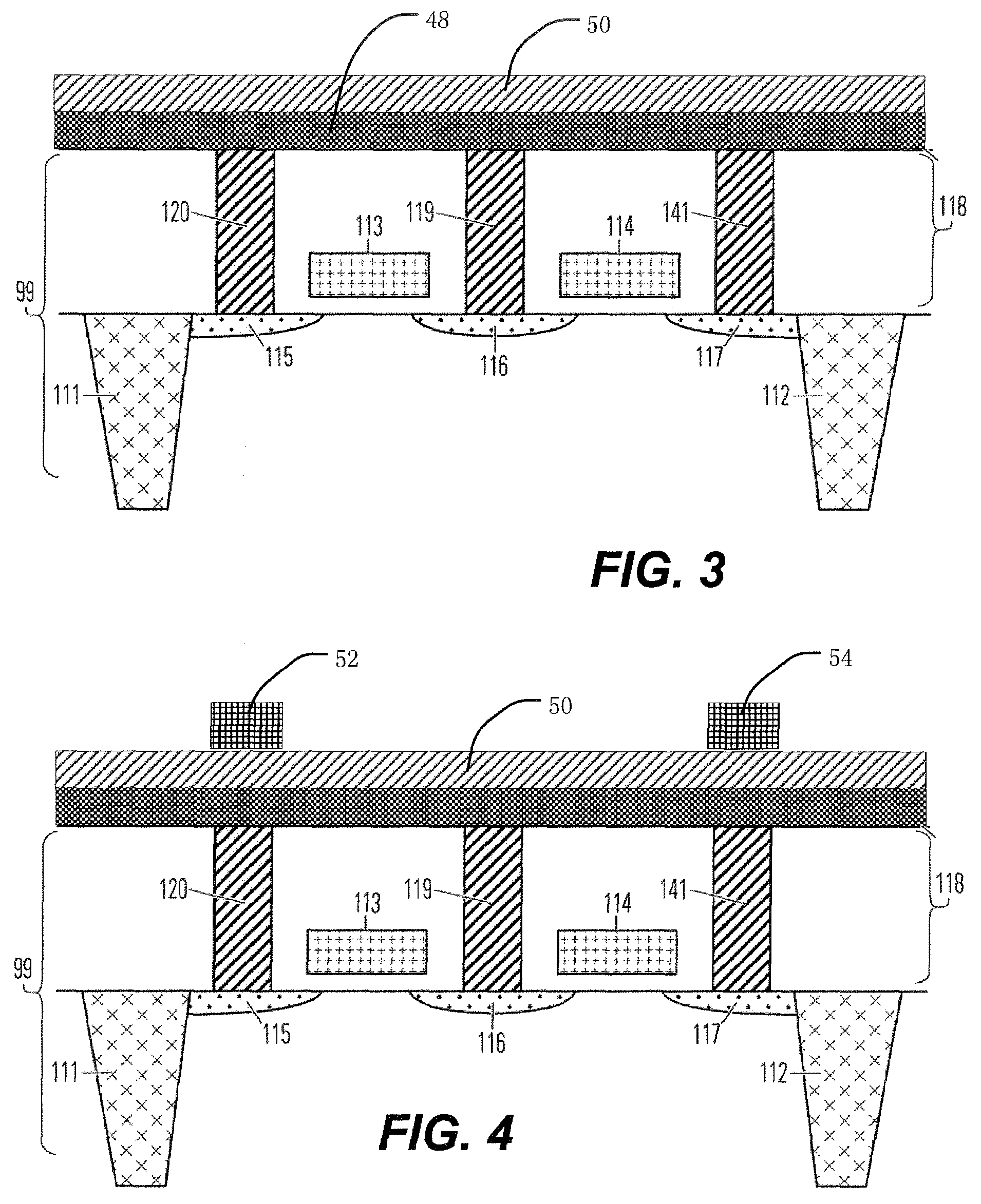
[0025]A detailed description of thin film fuse phase change memory cells, arrays of such memory cells, and methods for manufacturing such memory cells, is provided with reference to FIGS. 1-15.

[0026]FIG. 1 illustrates a basic structure of a memory cell 10 including a pillar of memory material 12 on a first electrode 14, a second electrode 16 including a conductive pillar 18, a shrinkable layer 20 surrounding the memory material 12 which is preferably a dielectric material or other material more resistive than that of the programmable resistive material in its high resistance state, dielectric material 22 (also called “dielectric fill-in material”), and a circumferential gap 24 formed in the shrinkable layer next to the pillar of memory material 12. The gap is a void in the shrinkable layer 20 that is self-forming, and thereby self-aligned.

[0027]In a particular embodiment, the memory material is a programmable resistive material that forms an inter-electrode current path and changes ...


PUM


Abstract

A memory device has a first electrode, a second electrode, and memory material defining an inter-electrode current path between the first electrode and the second electrode. A gap is formed by shrinkage of the shrinkable material between the memory material and a shrinkable material next to the memory material.

Description

[0001]International Business Machines Corporation, a New York corporation; Macronix International Corporation, Ltd., a Taiwan corporation, and Qimonda corporation, are parties to a Joint Research Agreement.BACKGROUND OF THE INVENTION[0002]1. Field of the Invention[0003]The present invention relates to resistively programmable materials, such as phase change based memory materials, including chalcogenide based materials and other materials, and to methods for manufacturing such devices.[0004]2. Description of Related Art[0005]Phase change based memory materials are widely used in read-write optical disks. These materials have at least two solid phases, including for example a generally amorphous solid phase and a generally crystalline solid phase. Laser pulses are used in read-write optical disks to switch between phases and to read the optical properties of the material after the phase change.[0006]Phase change based memory materials, like chalcogenide based materials and similar ma...

Claims


Application Information

Patent Timeline
IPC IPC(8): H01L47/00
CPCH01L45/06H01L45/1226H01L45/1233H01L27/2436H01L45/144H01L45/1675H01L45/1293H10B63/30H10N70/231H10N70/823H10N70/8616H10N70/826H10N70/8828H10N70/063
Inventor LUNG, HSIANG LAN
Owner MACRONIX INT CO LTD
Why Eureka
Try Eureka