Organic light emitting device, method of manufacturing the same, and method of forming organic layer

Active Publication Date: 2008-08-21
SAMSUNG DISPLAY CO LTD
View PDF5 Cites 3 Cited by
  • Summary
  • Abstract
  • Description
  • Claims
  • Application Information

AI Technical Summary

Benefits of technology

[0008]Aspects of embodiments of the present invention are directed toward an organic light emitting device that has long lifespan by improving the characteristics of an interface between an emissive layer (e.g., at least one of a red emissive layer, a green emissive layer, or a blue emissive layer) and an electron transport layer, a method of manufacturing the organic light emitting device, and a method of forming an organic layer having a multilayer structure.
[0022]The organic light emitting device according to an embodiment as described above has improved lifespan properties.

Problems solved by technology

However, a conventional organic light emitting device does not have satisfactory lifespan properties, and thus there is a need for further improvement.

Method used


Image

  • Organic light emitting device, method of manufacturing the same, and method of forming organic layer
  • Organic light emitting device, method of manufacturing the same, and method of forming organic layer
  • Organic light emitting device, method of manufacturing the same, and method of forming organic layer

Examples


Embodiment Construction

[0027]In the following detailed description, only certain exemplary embodiments of the present invention are shown and described, by way of illustration. As those skilled in the art would recognize, the invention may be embodied in many different forms and should not be construed as being limited to the embodiments set forth herein. Also, in the context of the present application, when an element is referred to as being “on” another element, it can be directly on the another element or be indirectly on the another element with one or more intervening elements interposed therebetween. Like reference numerals designate like elements throughout the specification.

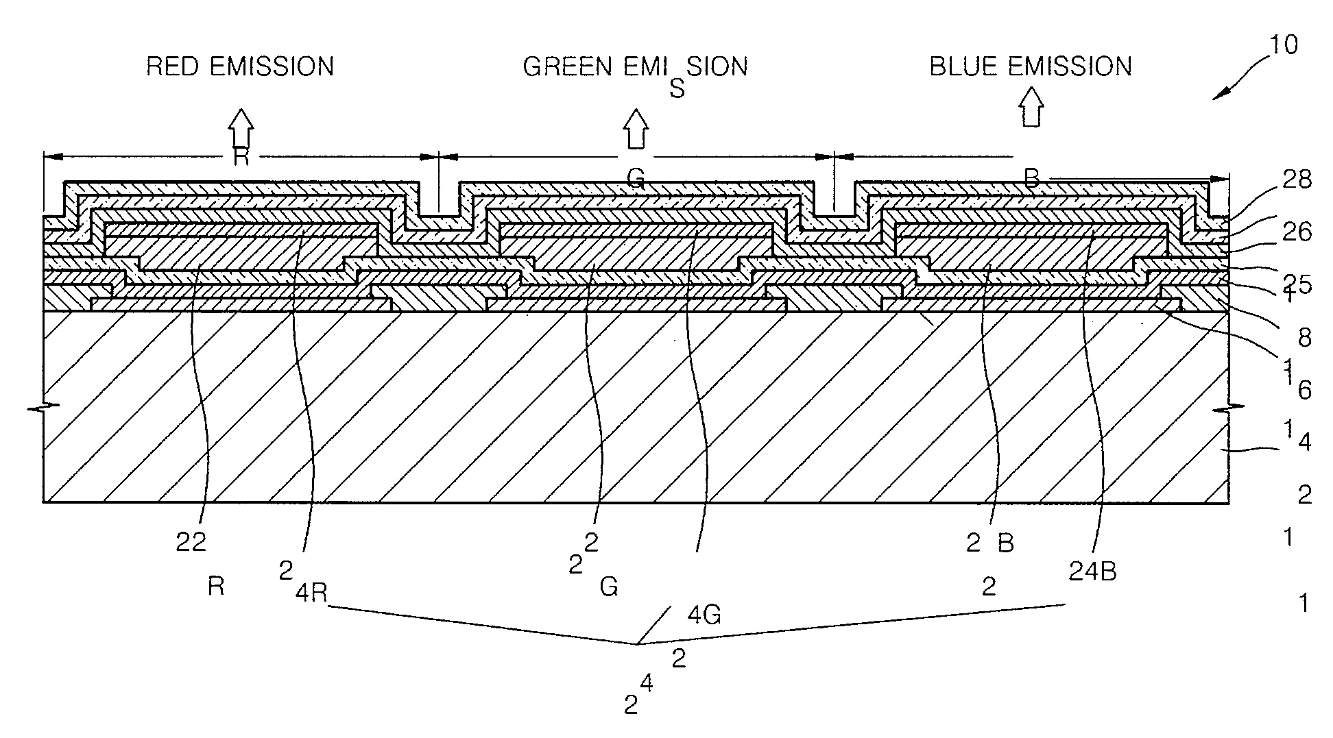
[0028]FIG. 1 is a schematic cross-sectional view of an organic light emitting device 10 according to an embodiment of the present invention.

[0029]Referring to FIG. 1, the organic light emitting device 10 includes a substrate 11, first electrodes 12, a hole injection layer 16 and a hole transport layer 18. In addition, a red emi...


PUM


Abstract

An organic light emitting device that has improved lifespan properties by improving the characteristics of an interface between at least one of a red emissive layer, a green emissive layer or a blue emissive layer, and an electron transport layer, and a method of manufacturing the organic light emitting device.

Description

CROSS-REFERENCE TO RELATED PATENT APPLICATION[0001]This application claims priority to and the benefit of Korean Patent Application No. 10-2007-0017086, filed on Feb. 20, 2007, in the Korean Intellectual Property Office, the entire content of which is incorporated herein by reference.BACKGROUND OF THE INVENTION[0002]1. Field of the Invention[0003]The present invention relates to an organic light emitting device, a method of manufacturing the same, and a method of forming an organic layer.[0004]2. Description of the Related Art[0005]An organic light emitting device is a self-emitting device that has a wide viewing angle, excellent contrast, and quick response time. Also, a lot of research has been conducted on organic light emitting devices because of their lower driving voltages and quicker response times, and because they can realize multicolor images.[0006]A conventional organic light emitting device has a stacked structure in the form of an anode / emissive layer / cathode structure....

Claims


Application Information

Patent Timeline
IPC IPC(8): H01J1/62B05D5/12
CPCC09K11/06C09K2211/1007C09K2211/1029C09K2211/1044H05B33/14C09K2211/185H01L27/3211H01L51/5048C09K2211/1092H10K59/35H10K50/14F24H7/04F24H9/0015F24H9/2035F24H1/52
Inventor YOON, JI-HWAN
Owner SAMSUNG DISPLAY CO LTD
Why Eureka
Try Eureka