Optical polarizer with nanotube array

a technology of optical polarizers and nanotubes, applied in the field of semiconductor fabrication, can solve the problems of reducing the quality of polarized light provided by the polarizer, becoming more difficult to print high-contrast images on the semiconductor wafer during lithographic processing,

Active Publication Date: 2008-08-21
GLOBALFOUNDRIES US INC
View PDF12 Cites 70 Cited by
  • Summary
  • Abstract
  • Description
  • Claims
  • Application Information

AI Technical Summary

Benefits of technology

[0004]An optical polarizer with nanotube array, substantially as shown in and / or described in connection with at least one of the figures, as set forth more completely in the claims.

Problems solved by technology

As pattern size continues to decrease in advanced wafer fabrication processes, it becomes more difficult to print a high-contrast image on the semiconductor wafer during lithographic processing.
However, conventional optical polarizers can allow an undesirable percentage of the blocked component of incident unpolarized light to pass through the polarizer, which decreases the quality of the polarized light provided by the polarizer.

Method used


Image

  • Optical polarizer with nanotube array
  • Optical polarizer with nanotube array
  • Optical polarizer with nanotube array

Examples


Embodiment Construction

[0010]The present invention is directed to an optical polarizer with nanotube array. The following description contains specific information pertaining to the implementation of the present invention. One skilled in the art will recognize that the present invention may be implemented in a manner different from that specifically discussed in the present application. Moreover, some of the specific details of the invention are not discussed in order not to obscure the invention.

[0011]The drawings in the present application and their accompanying detailed description are directed to merely exemplary embodiments of the invention. To maintain brevity, other embodiments of the present invention are not specifically described in the present application and are not specifically illustrated by the present drawings.

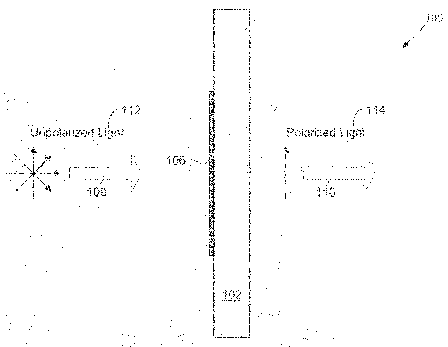
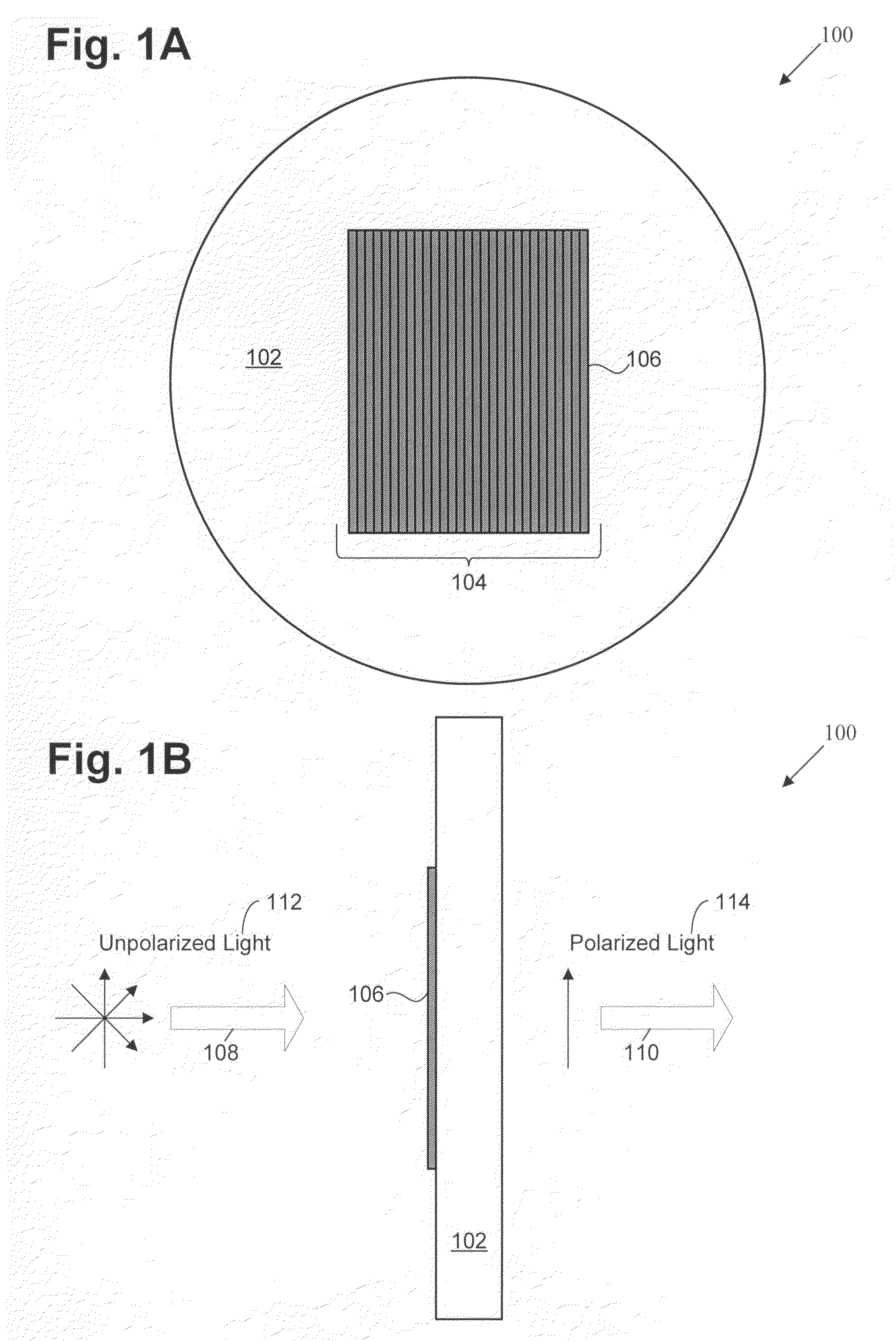
[0012]FIG. 1A shows a top view of optical polarizer 100, according to one embodiment of the present invention. In FIG. 1A, optical polarizer 100 includes substrate 102 and nanotube a...


PUM


Abstract

According to one exemplary embodiment, an optical polarizer positioned before a light source for use in semiconductor wafer lithography includes an array of aligned nanotubes. The array of aligned nanotubes cause light emitted from the light source and incident on the array of aligned nanotubes to be converted into polarized light for use in the semiconductor wafer lithography. The amount of polarization can be controlled by a voltage source coupled to the array of aligned nanotubes. Chromogenic material of a light filtering layer can vary the wavelength of the polarized light transmitted through the array of aligned nanotubes.

Description

1. TECHNICAL FIELD[0001]The present invention is generally in the field of semiconductor fabrication. More particularly, the invention is in the field of optical polarizers utilized in semiconductor fabrication.2. BACKGROUND ART[0002]During semiconductor wafer fabrication, a lithographic process is typically utilized to transfer a pattern from a mask to the semiconductor wafer. As pattern size continues to decrease in advanced wafer fabrication processes, it becomes more difficult to print a high-contrast image on the semiconductor wafer during lithographic processing. One method of increasing the contrast of the image projected on the wafer utilizes polarized light for illumination in the lithographic process. Polarized light can be provided by utilizing an optical polarizer to polarize incident light that is in an unpolarized, i.e. a randomly polarized, state.[0003]An optical polarizer can provide polarized light by blocking either the transverse electric (TE) or transverse magnet...

Claims


Application Information

Patent Timeline
Patent Type & Authority Applications(United States)
IPC IPC(8): G02B5/30
CPCG02B5/3075G02B5/3058G03F7/70566G02F1/0136
Inventor LAFONTAINE, BRUNO M.KIM, RYOUNG-HANLEVINSON, HARRY J.OKOROANYANWU, UZODINMA
Owner GLOBALFOUNDRIES US INC
Why Eureka
Try Eureka