Clock buffer circuit of semiconductor device

a technology of clock buffer and semiconductor device, which is applied in the direction of generating/distributing signals, instruments, pulse techniques, etc., can solve the problems of duty distortion deteriorating the high-speed operation of a memory device, the dcc accuracy is reduced, and the characteristics of tr/tf may not be equal

Inactive Publication Date: 2008-08-21
SK HYNIX INC
View PDF8 Cites 22 Cited by
  • Summary
  • Abstract
  • Description
  • Claims
  • Application Information

AI Technical Summary

Problems solved by technology

However, in a practical chip, the tR / tF characteristics may not be equal due to various external environmental factors, as shown in FIG. 3.
This means a duty distortion due to buffering, which leads to an increase in external parameters to be corrected by the DCC, resulting in a reduction in accuracy of the DCC.
As a result, this duty distortion deteriorates the high-speed operation of a memory device.

Method used


Image

  • Clock buffer circuit of semiconductor device
  • Clock buffer circuit of semiconductor device
  • Clock buffer circuit of semiconductor device

Examples


Embodiment Construction

[0026]Preferred embodiments of the present invention will now be described in detail with reference to the accompanying drawings.

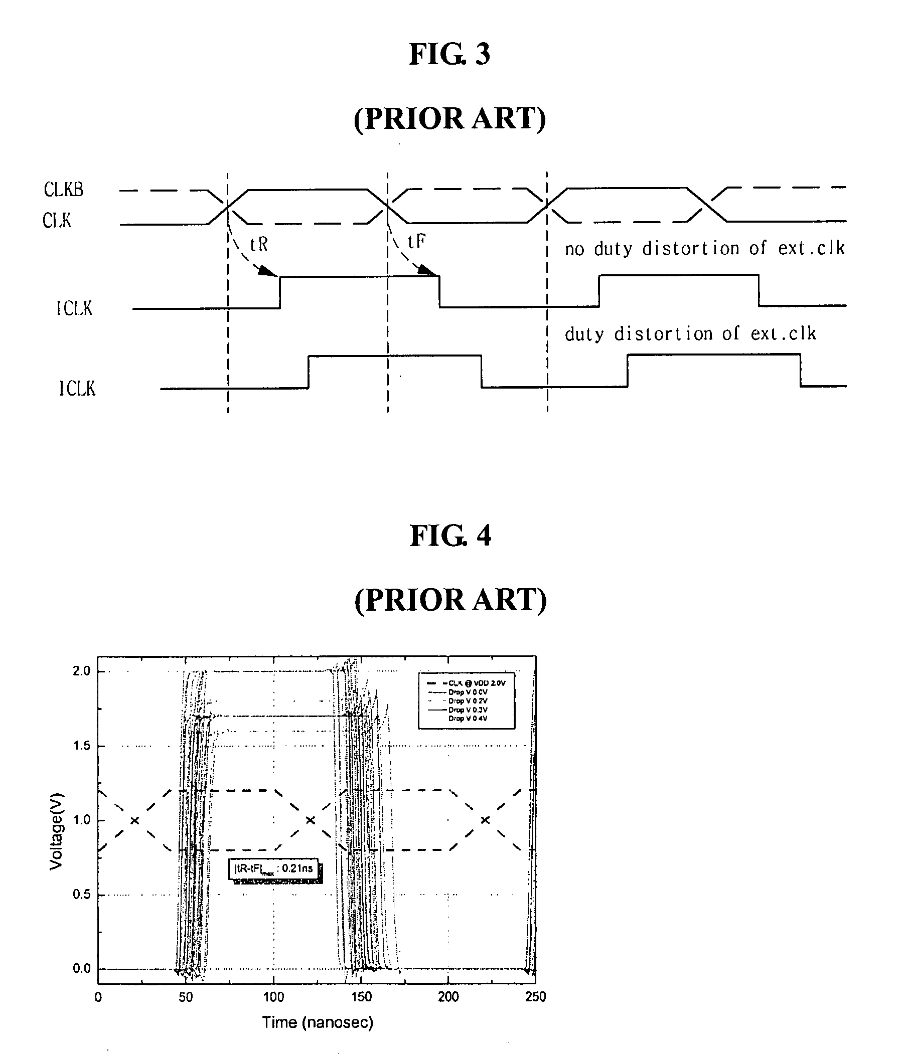
[0027]A clock buffer circuit of a semiconductor device according to the present invention is adapted to receive an external clock signal and generate an internal clock signal with no duty distortion, so that external parameters to be corrected by a duty correction circuit (DCC) can be reduced, resulting in an increase in accuracy of the DCC. Therefore, it is possible to improve the high-speed operation and reliability of a memory device.

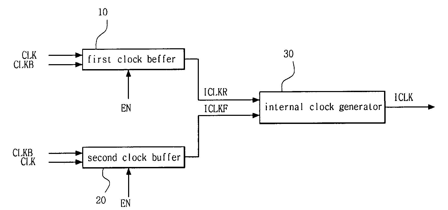
[0028]FIG. 5 is a block diagram showing the configuration of a clock buffer circuit according to an exemplary embodiment of the present invention, and FIG. 6 is a detailed circuit diagram of the clock buffer circuit of FIG. 5.

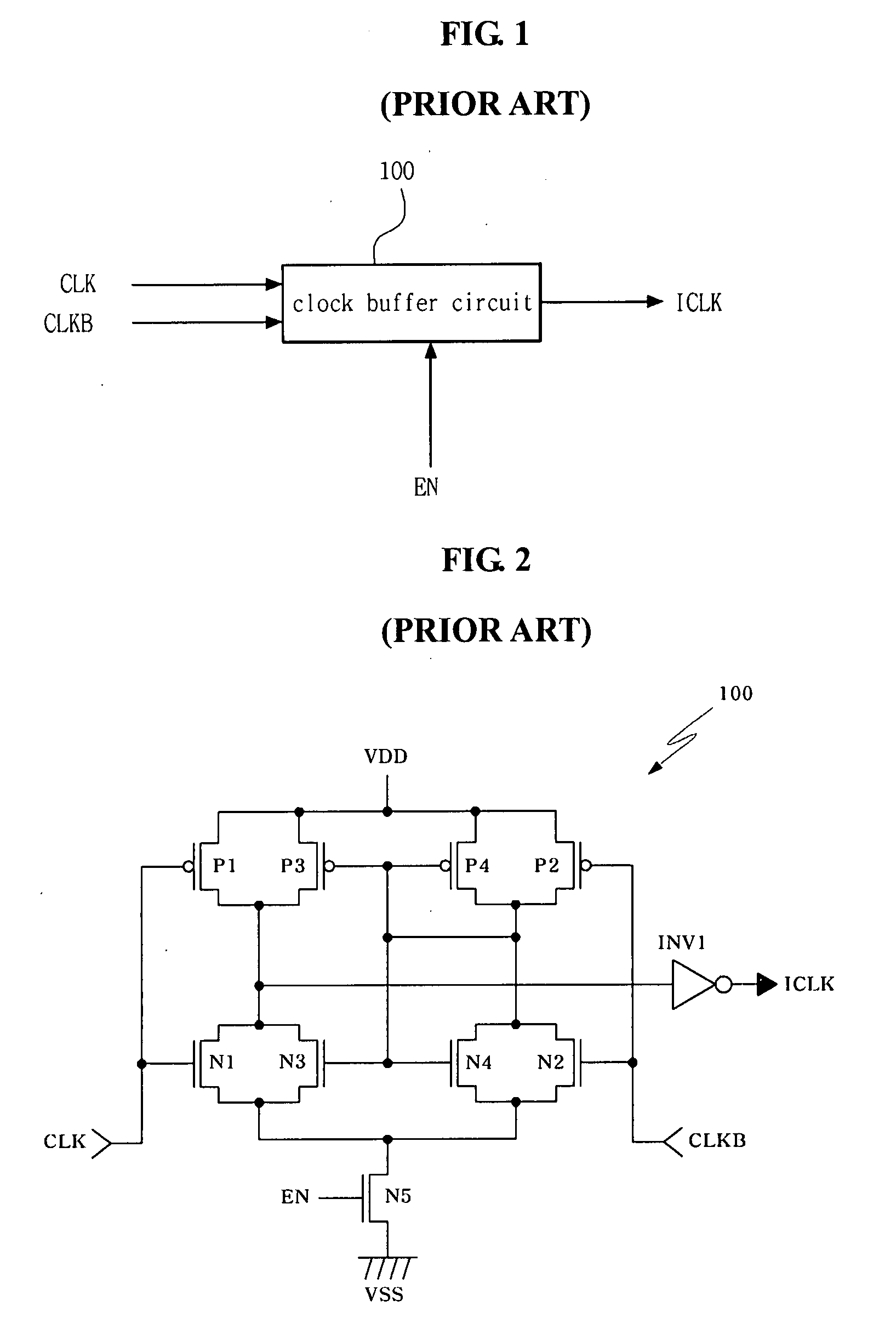
[0029]As shown in FIG. 5, the clock buffer circuit according to this embodiment comprises a first clock buffer 10 for receiving and buffering a normal-phase clock signal CLK, a second clock buffer 20 f...


PUM


Abstract

A clock buffer circuit of a semiconductor device is disclosed which receives an external clock signal and generates an internal clock signal with no duty distortion. The clock buffer circuit includes a first clock buffer for receiving and buffering a normal-phase clock signal, a second clock buffer for receiving and buffering a reverse-phase clock signal, and an internal clock generator for generating an internal clock signal in response to output signals from the first and second clock buffers.

Description

CROSS-REFERENCES TO RELATED APPLICATIONS[0001]The present application claims priority to Korean patent application number 10-2006-0138768, filed Dec. 29, 2006, which is incorporated by reference in its entirety.BACKGROUND OF THE INVENTION[0002]The present invention relates to a semiconductor device, and more particularly to a clock buffer circuit for buffering a clock signal.[0003]In general, a semiconductor memory device, such as a dynamic random access memory (DRAM), comprises a memory array including a plurality of memory cells for storing data.[0004]Particularly, in a synchronous DRAM (SDRAM) among various DRAMs, a data read / write operation is carried out synchronously with an external clock signal. For this reason, in the SDRAM, there is a need for a clock buffer circuit to generate an internal clock signal which is in synchronization with the external clock signal.[0005]The clock buffer circuit for the SDRAM employs a differential amplifier to which a clock signal and an inver...

Claims


Application Information

Patent Timeline
Patent Type & Authority Applications(United States)
IPC IPC(8): G06F1/04G06F1/12
CPCG11C7/22H03K5/1565G11C7/225G11C7/222G11C11/4076
Inventor CHO, KWANG JUN
Owner SK HYNIX INC
Why Eureka
Try Eureka