Quad flat no-lead chip carrier with stand-off

a flat no-lead, chip carrier technology, applied in the direction of printed circuit, sustainable manufacturing/processing, final product manufacturing, etc., can solve the problems of qfn misalignment with pcb pads, limit the ability of solder to wet, and affect the yield, so as to improve the yield of assembly to a substrate, improve the yield, and increase the solder area

Inactive Publication Date: 2008-08-28
GLOBALFOUNDRIES INC
View PDF9 Cites 5 Cited by
  • Summary
  • Abstract
  • Description
  • Claims
  • Application Information

AI Technical Summary

Benefits of technology

[0010]It is a further object of the present invention to provide a chip carrier which improves the yields in assembly to a substrate therefor.
[0011]It is yet a further object of the present invention to provide a QFN chip carrier with increased solder area for the leads and die pad, thereby providing improved solder joint strength when attached to a substrate, such as, a PCB.
[0012]It is yet another object of the present invention to provide a QFN chip carrier which attaches to a PCB, or the like, with improved solder joint reliability and yield.
[0013]It is yet another object of the present invention to provide a QFN chip carrier which connects to pads on a substrate through solder joints with improved fillets and higher stand-off.
[0014]In accordance with the present invention, a QFN chip carrier is provided with stand-offs which act to improve connection to a PCB, for example. The stand-offs take the form of rounded protrusions or bumps formed in the QFN leads and over the area of the die paddle. The rounded protrusions act to provide more QFN area for the solder to wet when the chip carrier is connected to pads on a PCB, for example. In addition, the rounded protrusions allow for formation of taller solder joints at QFN / PCB connection. The rounded protrusions may be formed by stamping dimples into the QFN copper plate used to form the leads and die paddle.
[0015]The rounded protrusions not only act to allow for higher solder joint thicknesses but also allow for the formation of better fillets. Not only is the strength of the solder joint improved but there is less possibility of shorting at QFN placement and reflow. Also, the process step of “picking and placing” the QFN into solder paste thickness results in less solder paste “push out” because of the rounded protrusions. In addition, with the rounded protrusion stand-offs, there is less floating of the QFN at reflow.

Problems solved by technology

Several problems arise as a result of the limited protrusion of stand-off of copper lead contacts 3 and die paddle 5 of leadframe 1.
For example, the limited protrusion limits the ability of the solder to wet due to the small area on the side of copper leads 6.
Yields are also affected due to the tendency of the QFN to float on the solder paste at assembly, which floating acts to cause the QFN to misalign with the PCB pads during solder reflow.

Method used


Image

  • Quad flat no-lead chip carrier with stand-off
  • Quad flat no-lead chip carrier with stand-off
  • Quad flat no-lead chip carrier with stand-off

Examples


Embodiment Construction

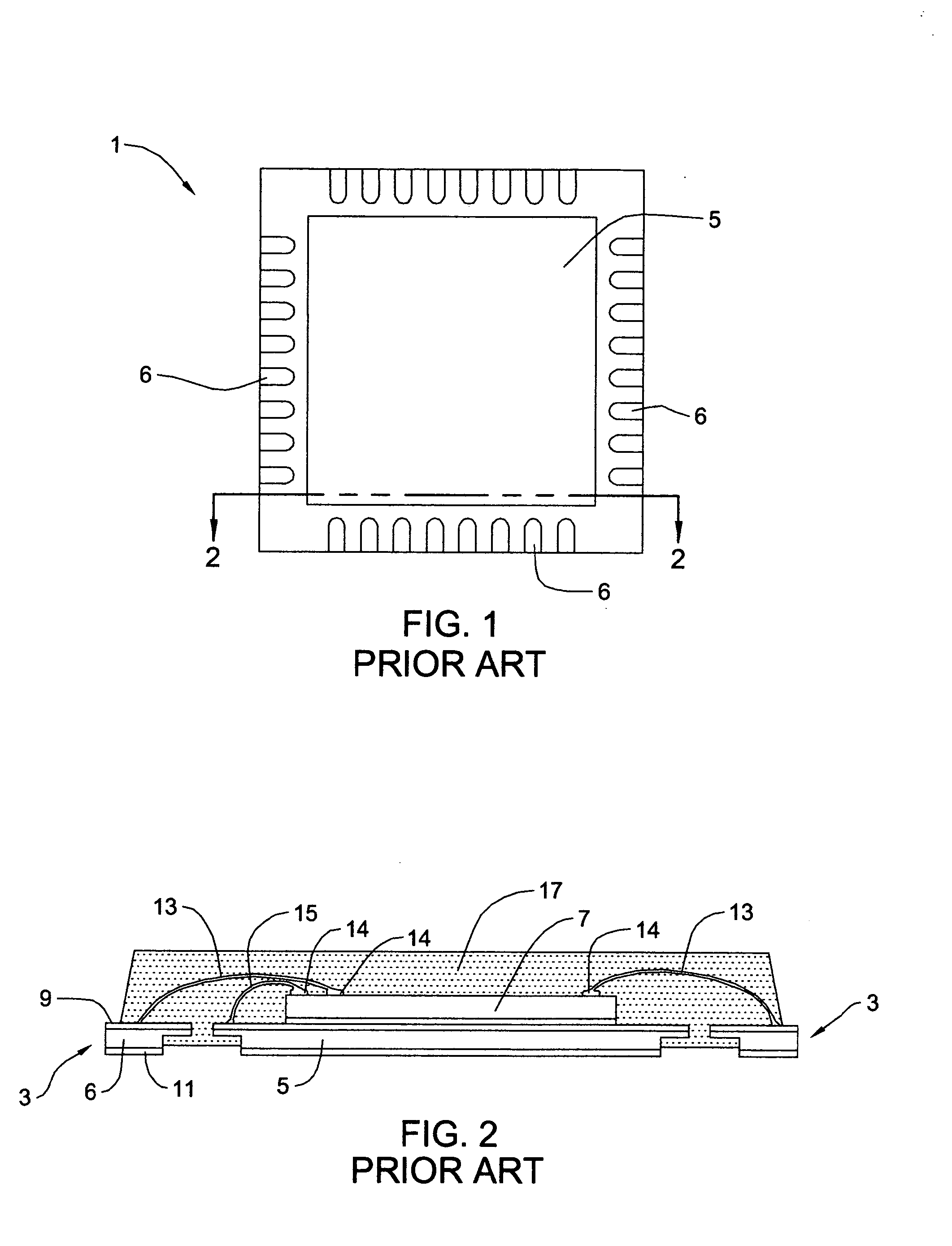
[0023]The bottom of a conventional QFN chip carrier is shown in FIG. 1. This is the side of the carrier that attaches to a substrate, such as, a PCB. Typically, the QFN chip carrier comprises a leadframe made from a flat copper plate. The leadframe 1 in FIG. 1 comprises a pattern that includes copper die paddle 5 and leads 6. The pattern of the paddle and leads may be etched or stamped out of the flat copper plate.

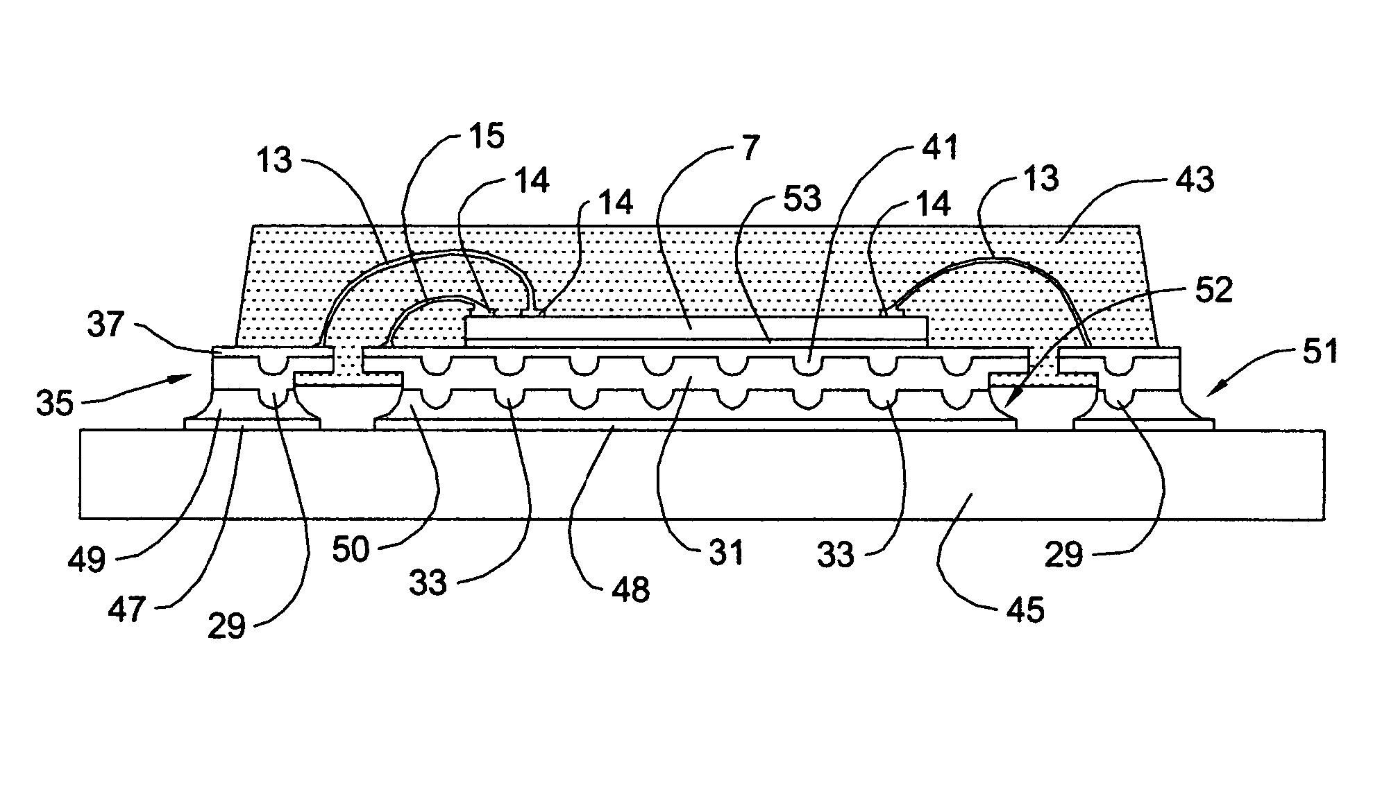
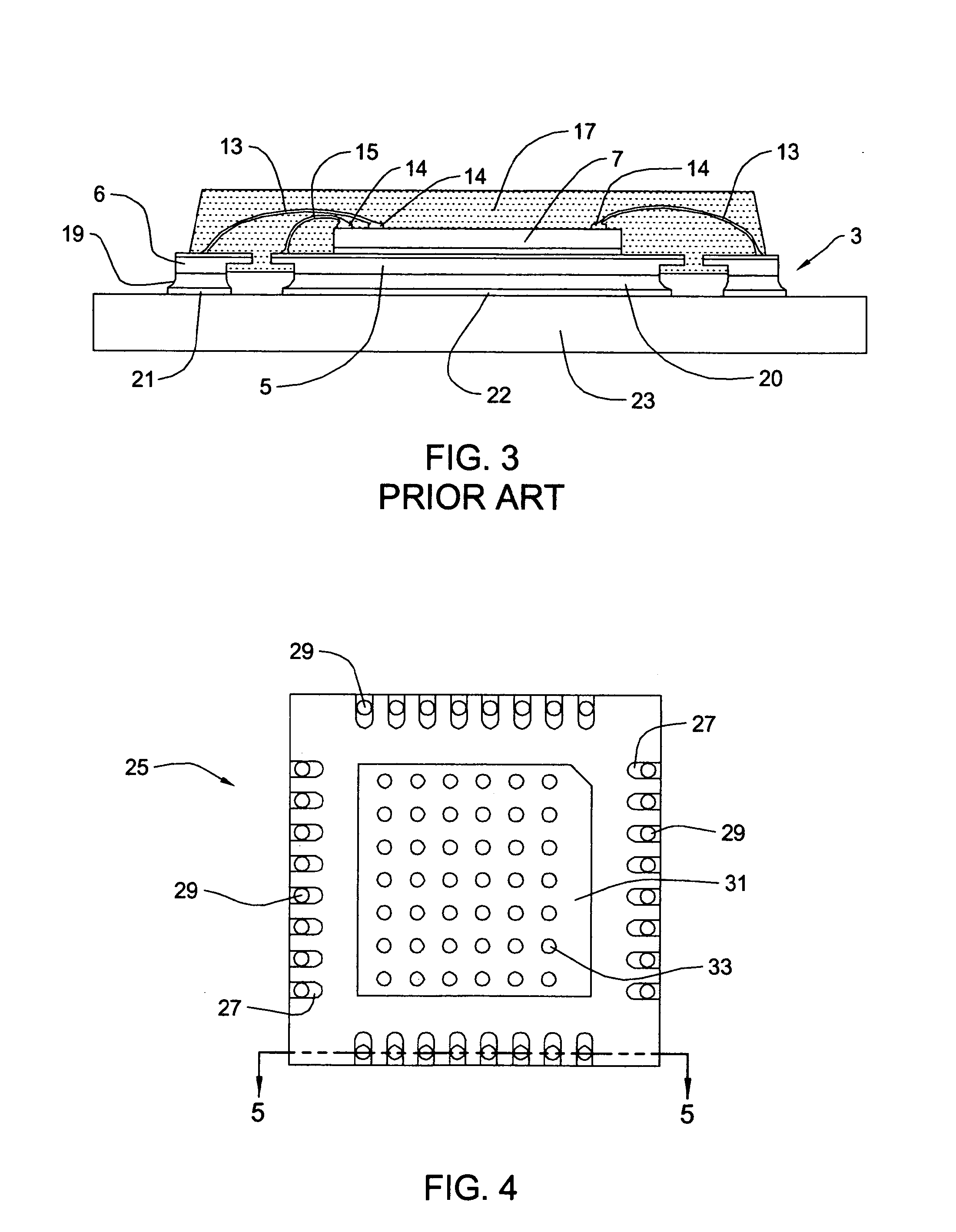
[0024]FIG. 2 shows a cross-sectional view of the QFN chip carrier of FIG. 1 taken along line 2-2. As shown, copper leads 6 are plated on the top with a layer 9 of, for example, silver and on the bottom with a layer 11 of, for example, solder to thereby form lead contacts 3. In this regard, it can be seen that the surfaces of die paddle 5 are also similarly plated on top and bottom at the same time leads 6 are plated. Wires 13, made of gold for example, connect contact pads 14 on chip 7 to lead contacts 3. Similarly, gold wire 15 forms a ground connection. As shown, this as...


PUM


Abstract

A QFN package with improved joint solder thickness for improved second level attachment fatigue life. The copper leadframe of a QFN chip carrier is provided with rounded protrusions in both the chip attach pad region and the surrounding lead regions before second level attachment. The rounded stand-off protrusions are formed from the copper itself of the copper of the leadframe. This may be achieved by punching dimples into one surface of the copper plate of the leadframe before plating to form protrusions on the opposing surface. This method of forming the rounded protrusions simplifies the process of forming stand-offs. The protrusions provide a structure that increases wetting area and allows the use of a larger quantity of solder for increased solder joint thickness and better die paddle solder joint area coverage. As a result of the increased solder joint thickness, second level fatigue life is significantly improved. As a result of the improved die paddle solder joint area coverage, improved thermal performance of the chip carrier is also significantly improved.

Description

BACKGROUND OF THE INVENTION[0001]1. Field of the Invention[0002]The present invention relates to chip carriers. More particularly, the present invention relates to quad flat no-lead (QFN) chip carriers and chip package structures.[0003]2. Background And Related Art[0004]Semiconductor packages are known to take a variety of forms. Similarly, chip carriers used in semiconductor packages take a variety of forms. One type of chip package currently used employs a leadframe arrangement. According to the type of leads used in the leadframe, a quad flat package (QFP) can be divided into quad flat packages with I-type leads (QFI), quad flat packages with J-types leads (QFJ) and quad flat packages no-lead (QFN). Because the outer end of the leads of the leadframe are uniformly cut along the four edges of a chip package, this latter type of package is also referred to as a quad flat no-lead chip carrier.[0005]FIG. 1 shows a plan view of the bottom side of a conventional QFN chip carrier. This ...

Claims


Application Information

Patent Timeline
Patent Type & Authority Applications(United States)
IPC IPC(8): H01L23/495H01L21/56
CPCH01L23/3107H05K2201/2036H01L23/49548H01L23/49582H01L24/45H01L2224/45144H01L2224/48091H01L2224/48247H01L2224/48257H01L2224/73265H01L2924/01046H01L2924/01078H01L2924/01079H05K3/341H05K2201/0367H05K2201/0373H05K2201/10689H05K2201/10727H05K2201/10969H01L23/49503H01L2924/15747H01L2924/01028H01L2224/32245H01L24/48H01L2924/00014H01L2924/00H01L2924/181Y02P70/50H01L2924/18301H01L2924/00012
Inventor MALONEY, JOHN J.SMITH, ROBERT M.WILSON, CHARLES H.
Owner GLOBALFOUNDRIES INC
Why Eureka
Try Eureka