Optical scanning device and image forming apparatus

a scanning device and image forming technology, applied in the field of optical scanning devices and image forming apparatuses, can solve the problems of low durability of the apparatus, impaired image quality, uneven distribution of light beams reflected on the deflecting surface,

Inactive Publication Date: 2008-08-28
RICOH KK
View PDF21 Cites 29 Cited by
  • Summary
  • Abstract
  • Description
  • Claims
  • Application Information

AI Technical Summary

Benefits of technology

[0010]It is an object of the present invention to at least partially solve the problems in the conventional technology According to an aspect of the present invention, there is provided an optical scanning device. The optical scanning device includes a deflector that includes a deflecting surface for deflecting a plurality of light beams for scanning in a main scanning direction; and an image-forming optical system that focuses the light beams near the deflecting surface in a sub-scanning direction perpendicular to the main scanning direction. The image-forming optical system includes at least two elements having a positive power in the main scanning direction. The size of the deflecting surface in the main scanning direction is smaller than a width of a light flux of the light beams in the main scanning direction.
[0011]According to another aspect of the present invention, there is provided an optical scanning device. The optical scanning device includes a first optical system that includes a coupling lens that couples a plurality of light beams; a deflector that includes a deflecting surface for deflecting the light beams having passed through the coupling lens; and a second optical system that focuses the light beams deflected by the deflector on a to-be-scanned surface. The to-be-scanned surface includes a writing area that is scanned with the light beams from a write-start position to a write-end position in a main scanning direction. A focal length of the coupling lens with respect to a distance between the deflecting surface and the coupling lens is larger than 1 and smaller than 4. The size of the deflecting surface in the main scanning direction is smaller than a width of a light flux of the light beams in the main scanning direction. The above and other objects, features, advantages and technical and industrial significance of this invention will be better understood by reading the following detailed description of presently preferred embodiments of the invention, when considered in connection with the accompanying drawings.

Problems solved by technology

However, if the number of revolutions of the deflector increases, vibrations and noise occurring from its driving system increase and, power consumption also increases, resulting in low durability of the apparatus.
Besides, because high-image density and high-speed image output have a trade-off relation, if the number of revolutions of the deflector increases, image quality is impaired.
However, in the optical scanning device using an overfield optical system, the distribution of the light amount of the light beams reflected upon the deflecting surface is disadvantageously uneven.
Moreover, in the VCSEL explained above, for example, because the angle of light-beam divergence is small, the distribution of the light amount the light beams incident upon the deflecting surface is slightly uneven compared with an edge-emitting laser and the like.

Method used


Image

  • Optical scanning device and image forming apparatus
  • Optical scanning device and image forming apparatus
  • Optical scanning device and image forming apparatus

Examples


first embodiment

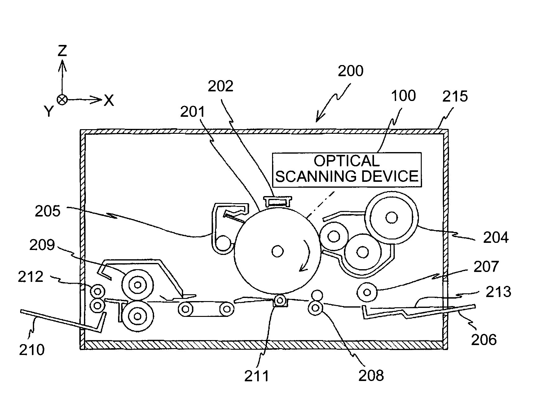
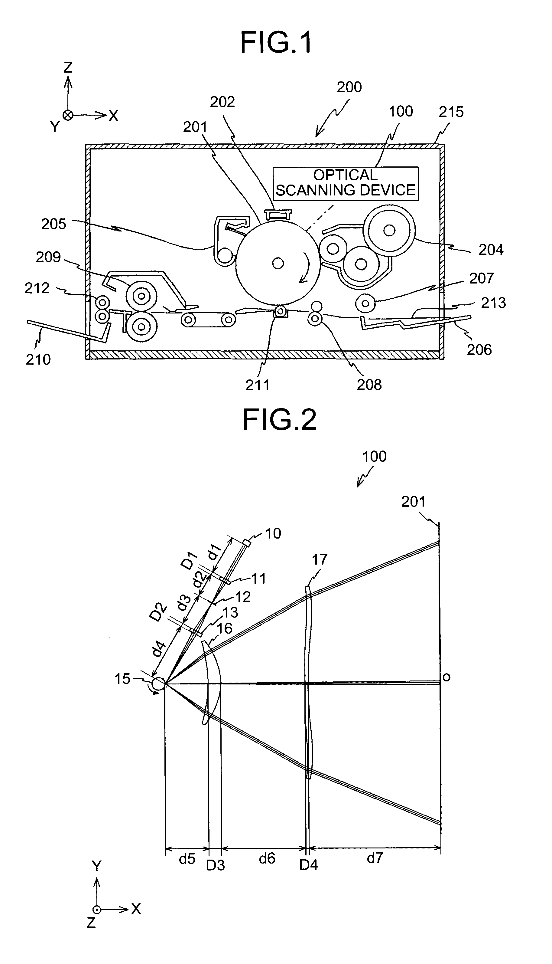
[0028]FIG. 1 is a schematic diagram of an image forming apparatus 200 according to the present invention.

[0029]The image forming apparatus 200 is explained as, for example, a printer that prints an image by using the Carlson process to transfer a toner image onto a recording medium (sheet). The image forming apparatus 200 includes an optical scanning device 100, a photosensitive drum 201, an electric charger 202, a toner cartridge 204, a cleaning case 205, a feed tray 206, a feed roller 207, a pair of registration rollers 208, a transfer charger 211, fixing rollers 209, eject rollers 212, an eject tray 210, and a housing 215 that accommodates these components.

[0030]The housing 215 has a substantially rectangular parallelepiped shape, and has formed on its +X side and −X side an opening communicating with an internal space.

[0031]The optical scanning device 100 is disposed in an upper position inside the housing 215, and deflects a light beam modulated based on image information to a ...

second embodiment

[0081]In the conventional optical systems, the focal depth is sufficiently ensured until Am is 2 micrometers, and fluctuations of the beam-spot diameter are not so large. However, when Am=4 micrometers or more, the focal depth is abruptly decreased in the main scanning direction, which causes the device to tend to have large fluctuations. On the other hand, in the optical system of the second embodiment, the focal depth is ensured until Am=6, and an increase in beam-spot diameter is within a tolerable range.

[0082]Thus, an optical system with a low lateral magnification is required for a light source with a near-field pattern of several micrometers or more. Because of this, as for at least one of a direction corresponding to the sub-scanning direction and a direction corresponding to the main scanning direction, the following Equation (1) is preferably satisfied:

{(ω / β·A)2−½}−2<0.7   (1)

where A is a near-field pattern, β is a lateral magnification of the entire optical system includin...


PUM


Abstract

An optical scanning device includes a light source, a deflector, and an image-forming optical system. The deflector includes a deflecting surface for deflecting light beams in a main scanning direction. The image-forming optical system includes two relay lenses having a positive power in the main scanning direction. The relay lenses cause main light beams of light beams emitted from the light source to cross near the deflecting surface in the main scanning direction.

Description

CROSS-REFERENCE TO RELATED APPLICATIONS[0001]The present application claims priority to and incorporates by reference the entire contents of Japanese priority documents 2007-048207 filed in Japan on Feb. 28, 2007 and 2007-147936 filed in Japan on Jun. 4, 2007.BACKGROUND OF THE INVENTION[0002]1. Field of the Invention[0003]The present invention relates to an optical scanning devices and an image forming apparatus.[0004]2. Description of the Related Art[0005]As an example of an image forming apparatus that forms an image by using the Carlson process, an image forming apparatus has been known in which, a surface of a rotating photosensitive drum is scanned with light beams to form a latent image thereon and a toner image developed from the latent image is fixed onto a sheet as a recording medium to form an image. In recent years, image forming apparatuses of this type have been often used for quick printing as an on-demand printing system, and there have been ever increasing demands fo...

Claims


Application Information

Patent Timeline
Patent Type & Authority Applications(United States)
IPC IPC(8): G02B26/10
CPCG02B26/12G02B26/123H04N1/0283H04N1/0301H04N1/047H04N2201/02497H04N2201/02456H04N2201/02458H04N2201/0246H04N2201/02462H04N1/12
Inventor WATANABE, NAOTOHAYASHI, YOSHINORI
Owner RICOH KK
Why Eureka
Try Eureka