Optical scanning device and image forming apparatus

a scanning device and image forming technology, applied in the field of optical scanning devices and image forming apparatuses, can solve the problems of deteriorating image quality, aforementioned problems becoming more serious, and thus deteriorating image quality

Inactive Publication Date: 2008-08-28
RICOH KK
View PDF19 Cites 34 Cited by
  • Summary
  • Abstract
  • Description
  • Claims
  • Application Information

AI Technical Summary

Benefits of technology

[0021]It is an object of the present invention to at lea...

Problems solved by technology

The configuration of the curvature then varies from one scanning line to another and the image quality is thus deteriorated.
Particularly, in full color image forming apparatuses that scanned surfaces for a plurality of colors are scanned by respective scanning optical systems and toner images corresponding to the respective colors are superimposed, for example, in tandem image forming apparatuses, the image quality can be deteriorated because of color shifts in the sub-scanning direction and differences in shading.
As the number of beams is increased, however, a region where emission points are arranged becomes large around the optical axis and the aforementioned problems become more serious.
Such color shift caused by the environmental changes is serious in image forming apparatuses with advanced high density and high image quality, particularly in color image forming apparatuses and measures needs to be taken.
All conditions including cost reduction in the apparatus, significantly high density image, and ensuring of...

Method used


Image

  • Optical scanning device and image forming apparatus
  • Optical scanning device and image forming apparatus
  • Optical scanning device and image forming apparatus

Examples


first embodiment

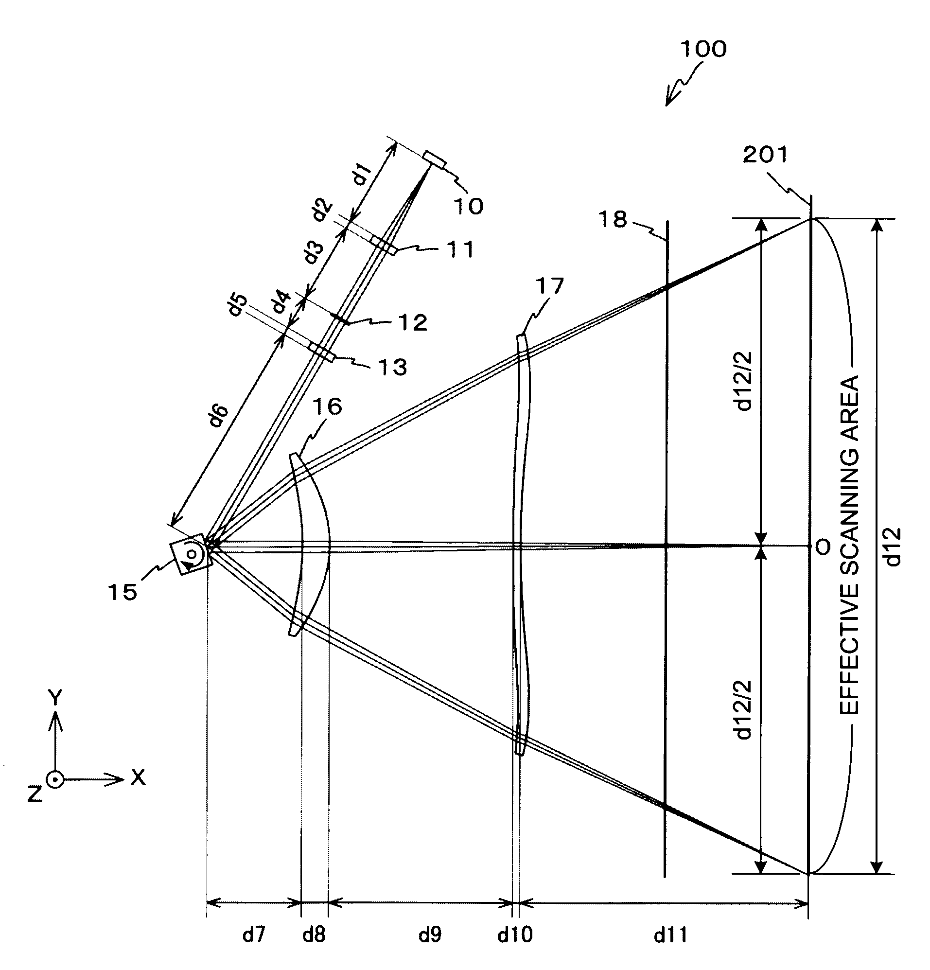
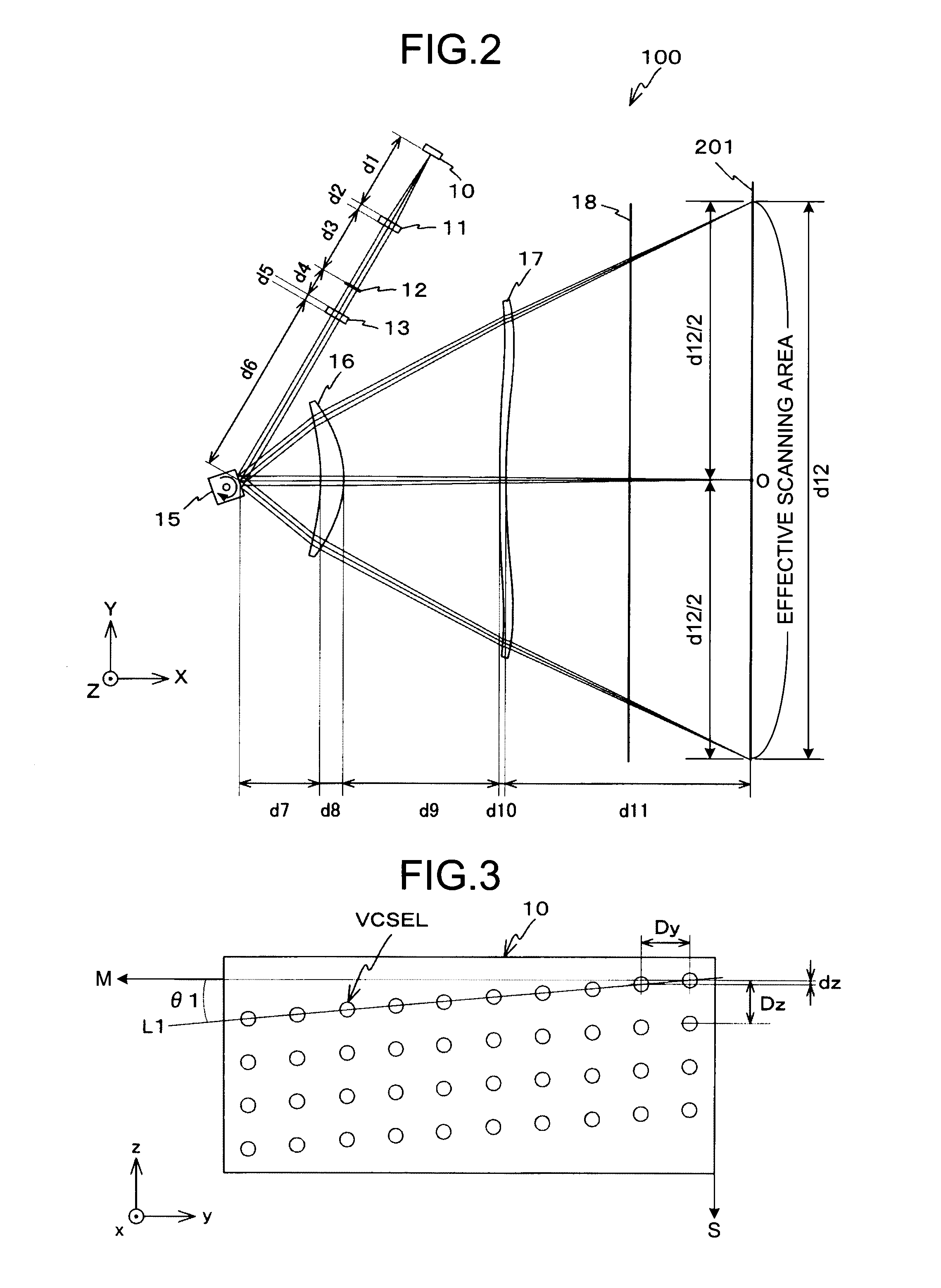
[0072]The light source 10 is a surface emitting semiconductor laser array that emission points, for example, VCSELs are two-dimensionally arranged. As shown in FIG. 3, on the light emitting surface (−X side surface), 40 VCSELs are arranged in a four-row, ten-column matrix whose row direction is parallel to the line L1 making an angle θ1 with the y axis and column direction is parallel to the z axis. Each VCSEL has a near-field pattern diameter of 4 micrometers. A light beam with a wavelength of 780 nanometers is outputted from VCSEL at 7±1 degrees of main scanning direction and sub-scanning direction divergence angles. In the first embodiment, the distance Dz between rows is 25.0 micrometers while the distance Dy between columns 30.0 micrometers. The distance dz between adjacent VCSELs in the Z-axis direction (sub-scanning direction) is 2.5 micrometers (4800 dots per inch (dpi)).

[0073]The coupling lens 11 has a focal length of 47.7 millimeters and couples the light beams from the li...

second embodiment

[0127]In the two-dimensional array of VCSELs, the distance between two adjacent light emitting units needs to be large in view of prevention of heat generation and wirings. The distance dz between two adjacent light emitting units in the S direction is 1=dz<5 μm. The distance dm between light emitting units in the M direction becomes larger than dz. for example, the writing density is 4800 dpi, Dy=30 μm, Dz=25 μm, and dz=2.5 μM. The distance between two light emitting units at the opposite ends in the M direction is calculated as Dy×9=270 μm, while the distance between two light emitting units at the opposite ends in the S direction dz×39=97.5 μm.

[0128]According to another example, in the two-dimensional array of VCSELs, the distance dz between two adjacent light emitting units in the S direction is determined to be 1=dz=4 μm. The distance dm between light emitting units in the M direction is larger than dz. According to the second embodiment, for example, the writing density is 48...


PUM


Abstract

By setting elements within the range that predetermined conditions are satisfied, for example, so that a size of a rotating polygon mirror is minimized, the rotating polygon mirror is made compact while the eclipse of light beams in the main scanning direction is prevented. The cost reduction of an apparatus is thus realized. The compact rotating polygon mirror reduces the consumption energy and the amount of heat generated in its drive system. Deteriorations in various optical characteristics including an increase in spot diameter of the light beam by temperature variation, uneven scanning pitch, and sub-scanning direction variation in beam pitch are suppressed.

Description

CROSS-REFERENCE TO RELATED APPLICATIONS[0001]The present application claims priority to and incorporates by reference the entire contents of Japanese priority documents 2007-048209 filed in Japan on Feb. 28, 2007, 2007-046451 filed in Japan on Feb. 27, 2007 and 2007-046442 filed in Japan on Feb. 27, 2007.BACKGROUND OF THE INVENTION[0002]1. Field of the Invention[0003]The present invention relates to an optical scanning device and an image forming apparatus.[0004]2. Description of the Related Art[0005]In current optical scanning devices and image forming apparatuses using such optical scanning devices, high quality images, full color images, high image forming speeds, and cost reductions in apparatuses have been demanded. To accomplish high quality images, curvature of scanning lines and variation in beam spot diameter on a scanned surface needs to be reduced. Moreover, position shifts of beam spots due to improvement in constant speed characteristic needs to be reduced.[0006]To acco...

Claims


Application Information

Patent Timeline
IPC IPC(8): G02B26/08
CPCB82Y20/00G02B26/123G02B26/125H01S5/423H01S5/3432H01S5/34326H01S5/4012H01S5/18311
Inventor ARAI, NOBUYUKIHAYASHI, YOSHINORIICHII, DAISUKE
Owner RICOH KK
Why Eureka
Try Eureka