Surface emitting laser array, production process thereof, and image forming apparatus having surface emitting laser array

a laser array and surface technology, applied in the direction of lasers, semiconductor laser arrangements, semiconductor lasers, etc., can solve the problems of difficult independent driving of devices, limited light output, and low light output, and achieve the effect of efficient heat dissipation

Inactive Publication Date: 2008-08-28
CANON KK
View PDF5 Cites 40 Cited by
  • Summary
  • Abstract
  • Description
  • Claims
  • Application Information

AI Technical Summary

Benefits of technology

[0013]In view of the above-described problems, it is thus an object of the present invention to provide a surface emitting laser array that can efficiently perform heat dissipation and independently drive the devices even wh

Problems solved by technology

On the other hand, the vertical cavity surface emitting laser involves a problem that saturation of light output is caused by temperature rise caused by generation of heat upon low-current driving compared with the edge-emitting type laser, and so the light output is limited.
In addition, the vertical cavity surface emitting laser also involves a problem that light output is lowered with rise of a peripheral temperature (environmental temperature) of a device.
When peripheral parts of a mesa structure of such a narrow-pitch laser are charged with a plated metal like Japanese Patent App

Method used


Image

  • Surface emitting laser array, production process thereof, and image forming apparatus having surface emitting laser array
  • Surface emitting laser array, production process thereof, and image forming apparatus having surface emitting laser array
  • Surface emitting laser array, production process thereof, and image forming apparatus having surface emitting laser array

Examples


example 1

[0032]In Example 1, a structural example of a vertical cavity surface emitting laser array constituted by applying the present invention is described.

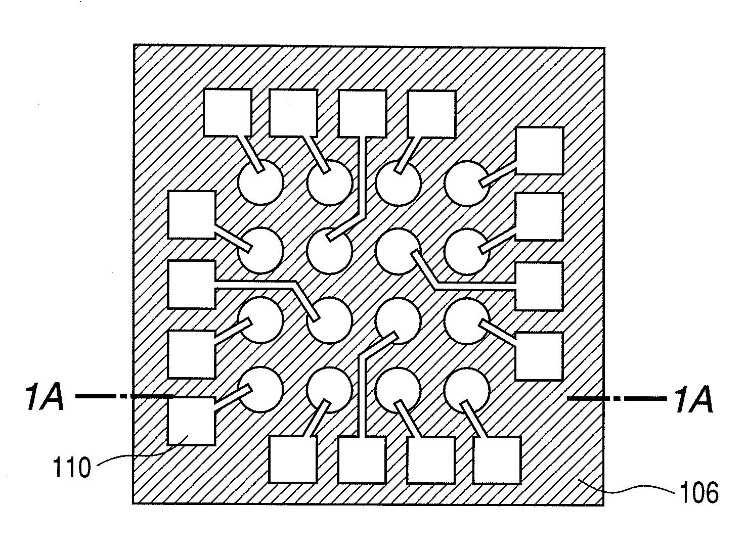
[0033]FIGS. 1 and 1A illustrate a vertical cavity surface emitting laser array according to this embodiment. FIG. 1A is a cross-sectional view taken along line 1A-1A in FIG. 1. A plurality of surface emitting laser devices is arranged in this surface emitting laser array.

[0034]In FIGS. 1 and 1A, a semiconductor layer 100 contains at least a first reflection mirror, an active layer, a current confined portion and a second reflection mirror, which are formed on a substrate.

[0035]In this embodiment, the first reflection mirror is comprised of a DBR mirror. In this embodiment, a first metal material layer is comprised of a metal material layer for heat dissipation indicated by ‘102’.

[0036]The laser array comprises a first insulating layer 104, a second insulating layer 106, the active layer 108, a metal material layer 110 for wiring and an...

example 2

[0060]In Example 2, a structural example of a vertical cavity surface emitting laser array according to another embodiment than the array of Example 1 constituted by applying the present invention is described. A difference of Example 2 from Example 1 resides in that the second insulating layer is formed only in regions in contact with the metal material layer for wiring.

[0061]FIGS. 3 and 3A illustrate the vertical cavity surface emitting laser array according to this embodiment. FIG. 3A is a cross-sectional view taken along line 3A-3A in FIG. 3.

[0062]In FIGS. 3 and 3A, a semiconductor layer 300, a metal material layer 302, a first insulating layer 304, second insulating layer 306, an active layer 308, a metal material layer 310 for wiring and an electrode 312 are illustrated.

[0063]In the vertical cavity surface emitting laser array according to this embodiment, the first insulating layer 304 is formed on the semiconductor layer 100 and portions other than the top surface of mesa st...

example 3

[0084]In Example 3, a structural example of an image forming apparatus having the vertical cavity surface emitting laser array according to the present invention is described.

[0085]FIGS. 5A and 5B illustrate structural drawings of an image forming apparatus of an electrophotographically recording system, in which the vertical cavity surface emitting laser array according to the present invention is mounted. FIG. 5A is a side elevation of the image forming apparatus, and FIG. 5B is a side elevation of the apparatus.

[0086]In FIGS. 5A and 5B, a photosensitive drum 500, a charger 502, a developer 504, a transfer charger 506, a fixer 508, a polygon mirror 510, a motor 512, the vertical cavity surface emitting laser array 514, a reflection mirror 516, a collimator lens 520 and an f-θ lens 522 are illustrated.

[0087]In FIGS. 5A and 5B, the motor 512 rotationally drives the polygon mirror 510. The polygon mirror 510 in this embodiment has six reflection surfaces. The vertical cavity surface ...


PUM


Abstract

A surface emitting laser array comprising a plurality of surface emitting laser devices each having a semiconductor layer containing a first reflection mirror, an active layer, a current confined portion and a second reflection mirror. The laser array further comprises a first metal material layer for dissipating heat formed through a first insulating layer on the semiconductor layer and a second metal material layer for injecting current into the active layer formed through a second insulating layer on the first metal material layer. The first metal material layer is commonly shared by the plurality of the surface emitting laser devices.

Description

BACKGROUND OF THE INVENTION[0001]1. Field of the Invention[0002]The present invention relates to a surface emitting laser array, a production process thereof, and an image forming apparatus having a surface emitting laser array.[0003]2. Description of the Related Art[0004]A vertical cavity surface emitting laser (VCSEL) is a laser capable of emitting light in a direction perpendicular to a substrate surface and has a feature that a two-dimensional array can be easily formed, which an edge-emitting type laser does not have.[0005]In particular, densification and faster operation can be simultaneously achieved by the parallel processing of multiple beams emitted from the two-dimensional array, and so it is expected to be used in various industrial applications. For example, when a vertical cavity surface emitting laser array is used as a light source for exposure of electrophotography, high-definition and faster printing can be achieved by parallel processing in a printing process by u...

Claims


Application Information

Patent Timeline
IPC IPC(8): H01S5/40H01L21/02H01S3/04
CPCH01S5/02276H01S5/423H01S5/0425H01S5/02469H01S5/04252H01S5/04256H01S5/02345
Inventor UCHIDA, TATSURO
Owner CANON KK
Why Eureka
Try Eureka