
Press-fit pin and board structure

a press-fit pin and board technology, applied in the direction of printed circuits, electrical devices, printed circuit aspects, etc., can solve the problems of increasing the demand for downsizing boards, transmission losses, and mismatching of impedances, so as to suppress the electrically-static capacitance of through-holes, reduce the number of wiring layers, and reduce the effect of downsizing boards

Inactive Publication Date: 2008-08-28
HITACHI LTD
View PDF12 Cites 53 Cited by
  • Summary
  • Abstract
  • Description
  • Claims
  • Application Information

AI Technical Summary

Benefits of technology

The present invention provides a printed wiring board with a through-hole that includes a signal transmission layer and a press-fit pin for connection to other components. The electrode in the through-hole is exposed and has a lock portion to securely fit into the through-hole. This design reduces signal transmission loss, maintains waveform quality, and allows for a smaller board size and increased wiring layers. The retaining force of the press-fit pin is also improved.

Problems solved by technology

Therefore, a high-speed serial transmission system has now become mainstream since a conventional parallel transmission system has the problem of a significant impact from “skew” in high rate (high-frequency) bands.
The above-described through-hole, which is provided on the board and into which the press-fit pin of the connector is fitted, has electrostatic capacitance, which causes impedance mismatching, particularly in the high rate bands.
This can potentially result in transmission loss due to signal skew.
On the other hand, the demand for downsizing a board has been increasing, and this had led to downsizing the through-holes themselves.
Also, the increase in density and number of layers of the board increasingly presents the problem of increased electrostatic capacitance in the through-holes.
Furthermore, the sufficient contact force between the press-fit pin and the through-hole may not be ensured by merely reducing the area of the electrode portion of the through-hole to suppress the electrostatic capacitance of the through-hole.
Thus, signal transmission loss is decreased even in the high rate bands.

Method used


Image

  • Press-fit pin and board structure
  • Press-fit pin and board structure
  • Press-fit pin and board structure

Examples


Embodiment Construction

[0030]An embodiment of this invention will be described with reference to the attached drawings.

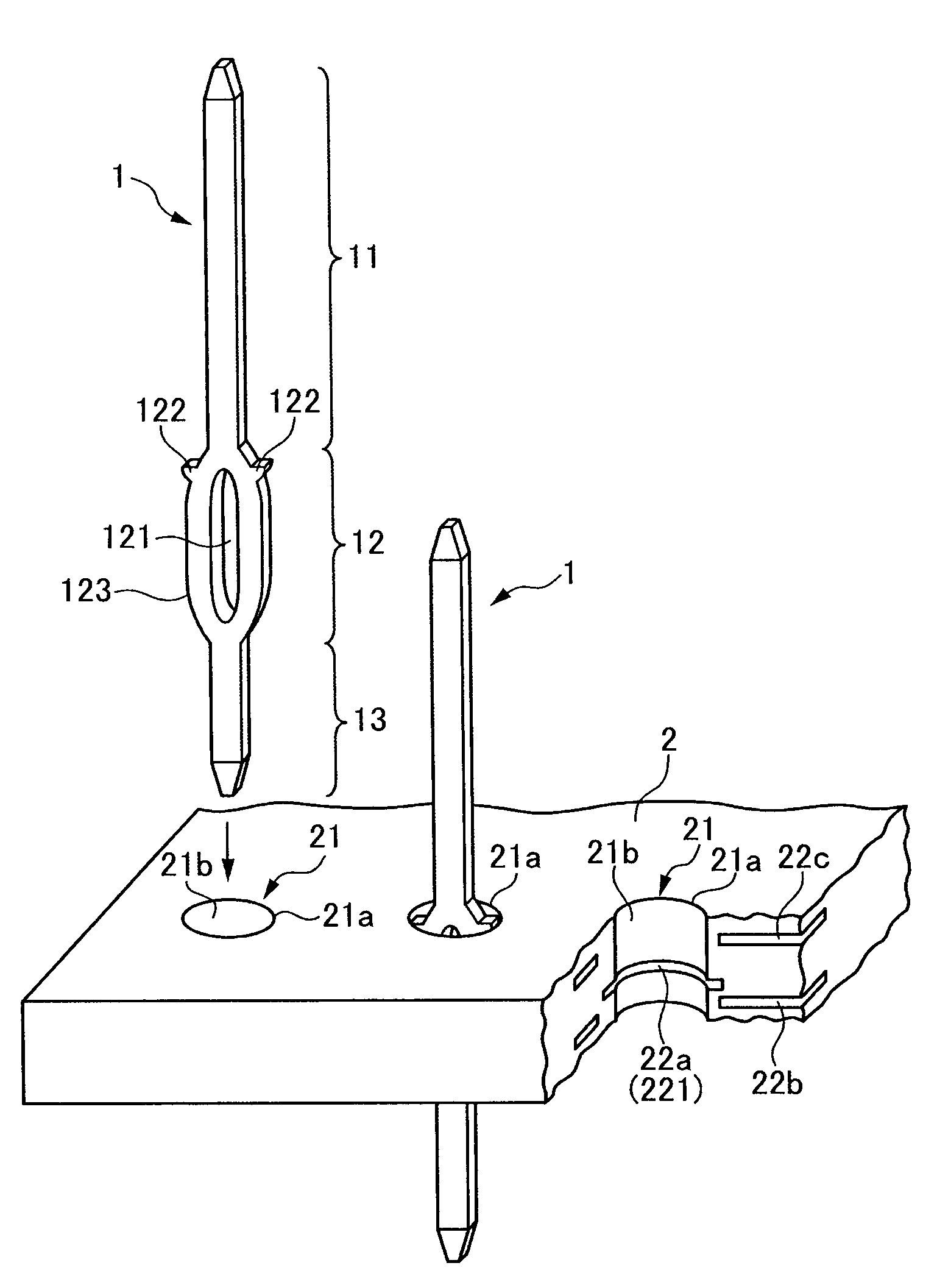
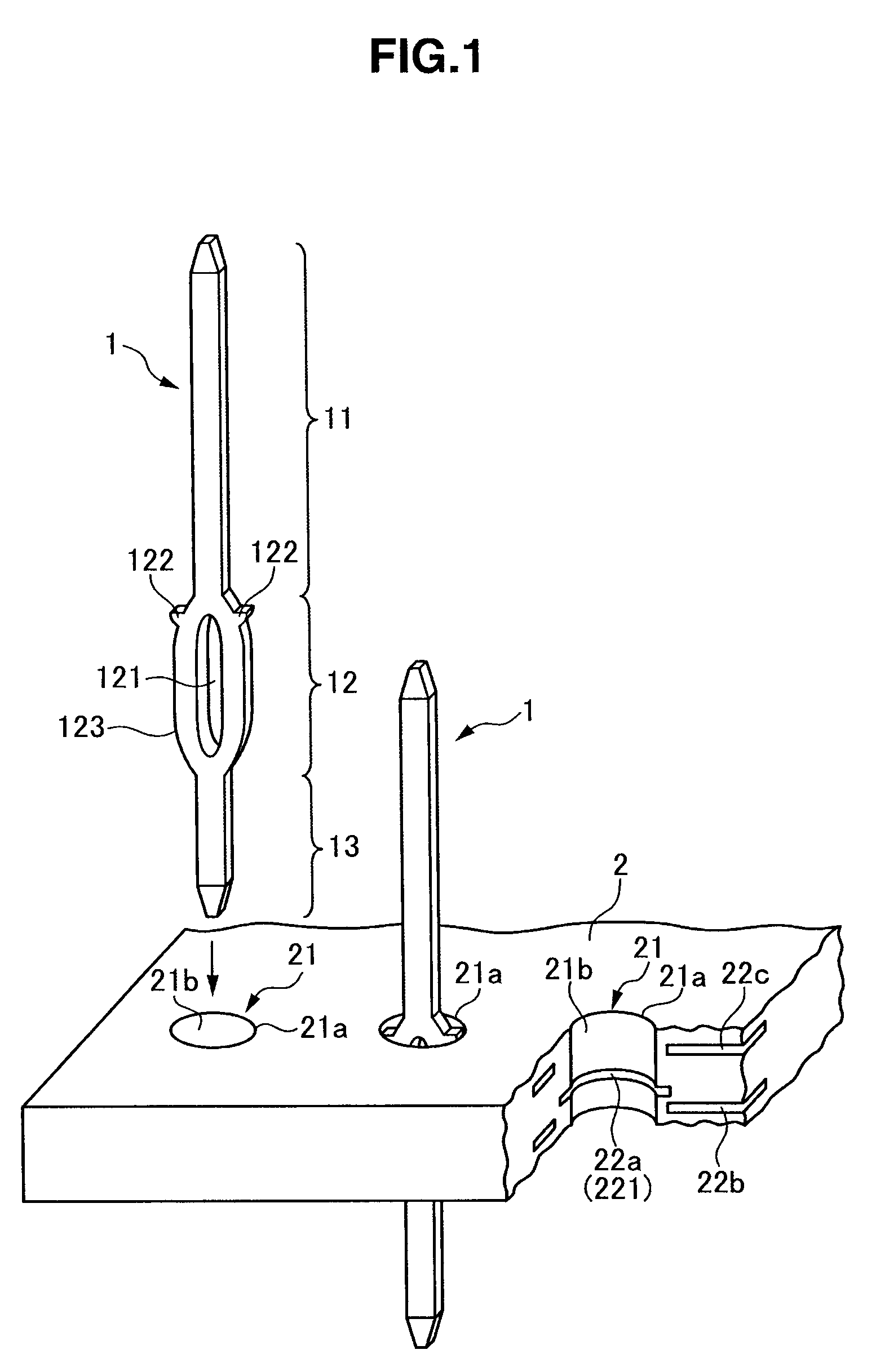
[0031]FIG. 1 is a partial perspective view showing press-fit pins 1 and a printed wiring board 2 according to an embodiment of the invention.

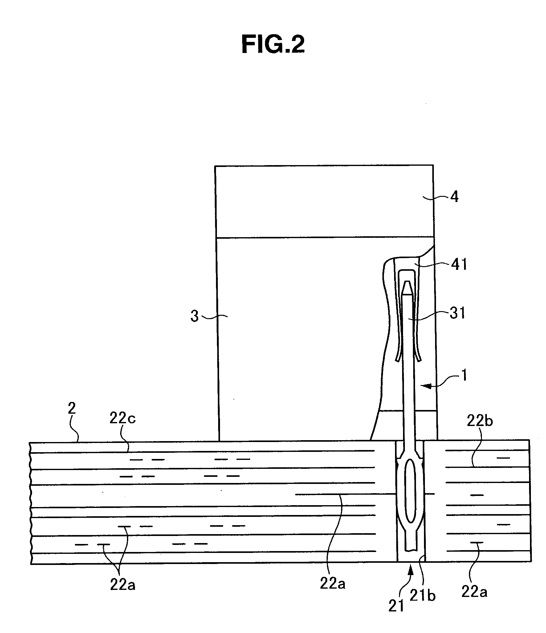
[0032]Referring to FIG. 1, press-fit pins 1 are press-fitted into through-holes 21 through opening portions 21a, which are formed in the printed wiring board 2, to be fixed to the printed wiring board 2. Each press-fit pin 1 fixed to the print wiring board 2 mechanically retains a housing of a plug connector 3 to serve as a terminal 31 of the plug connector 3 (see FIG. 2). The plug connector 3 is fitted with another connector (receptacle connector) 4, thereby allowing the terminal 31 and a terminal 41 of the respective connectors to be electrically connected with each other.

[0033]FIG. 3 is a diagram illustrating a product example using the printed wiring board 2 configured to include the press-fit pins 1 according to an embodiment of the invention. T...


PUM


Abstract

Provided is a printed wiring board formed with a through-hole into which a press-fit pin is press-fitted. The printed wiring board includes at least one signal transmission layer, a signal transmission wiring pattern formed in the signal transmission layer, and an electrode portion of the signal transmission wiring pattern exposed at an inner circumferential surface of the through-hole. The electrode portion is not formed covering the entire inner circumferential surface of the through-hole but at a part of the inner circumferential surface of the through-hole.

Description

CROSS-REFERENCES TO RELATED APPLICATIONS[0001]This application relates to and claims priority from Japanese Patent Application No. 2007-045850, filed on Feb. 26, 2007, the entire disclosure of which is incorporated herein by reference.BACKGROUND[0002]1. Field of the Invention[0003]The present invention relates to a junction technique using a press-fit pin, and in particular relates to a structure for a printed wiring board formed with a through-hole for press fitting of a press-fit pin.[0004]2. Description of Related Art[0005]A press-fit pin junction technique is a technique in which the press-fit pin, which is an acicular terminal given the property of compressive elasticity, is fitted into a through-hole in a printed wiring board to ensure a frictional force (retaining force), thereby being mechanically and electrically fixed to the printed wiring board. The press-fit pin may be called a compliant pin. A copper-plated electrode portion is formed on an inner circumferential surface...

Claims


Application Information

Patent Timeline
Patent Type & Authority Applications(United States)
IPC IPC(8): H01R12/00
CPCH01R12/585H05K3/308H05K3/325H05K2201/092H05K2201/10189H05K2201/10303H05K2201/1059H05K2201/10878
Inventor SUEYOSHI, JUNYA
Owner HITACHI LTD
Learn More