Circuit board surface structure and fabrication method thereof

a technology of circuit board and surface structure, which is applied in the direction of double resist layer, electrical apparatus construction details, and semiconductor/solid-state device details, etc., can solve the problem that the fine pitch requirement of advanced electronic products cannot be met, and the surface structure of the soldering pad cannot be easily formed, so as to achieve the effect of strengthening the bonding of conductive elements and being easy to attach

Active Publication Date: 2008-09-11
UNIMICRON TECH CORP
View PDF8 Cites 22 Cited by
  • Summary
  • Abstract
  • Description
  • Claims
  • Application Information

AI Technical Summary

Benefits of technology

[0021]Therefore, the fabrication method of a circuit board surface structure according to the present invention mainly comprises forming a first and a second insulating protective layers of different composition ratios on a surface of a circuit board having electrically connecting pads so as to make the first openings have bigger diameter than the second openings and make the first and second openings have positive taper sh

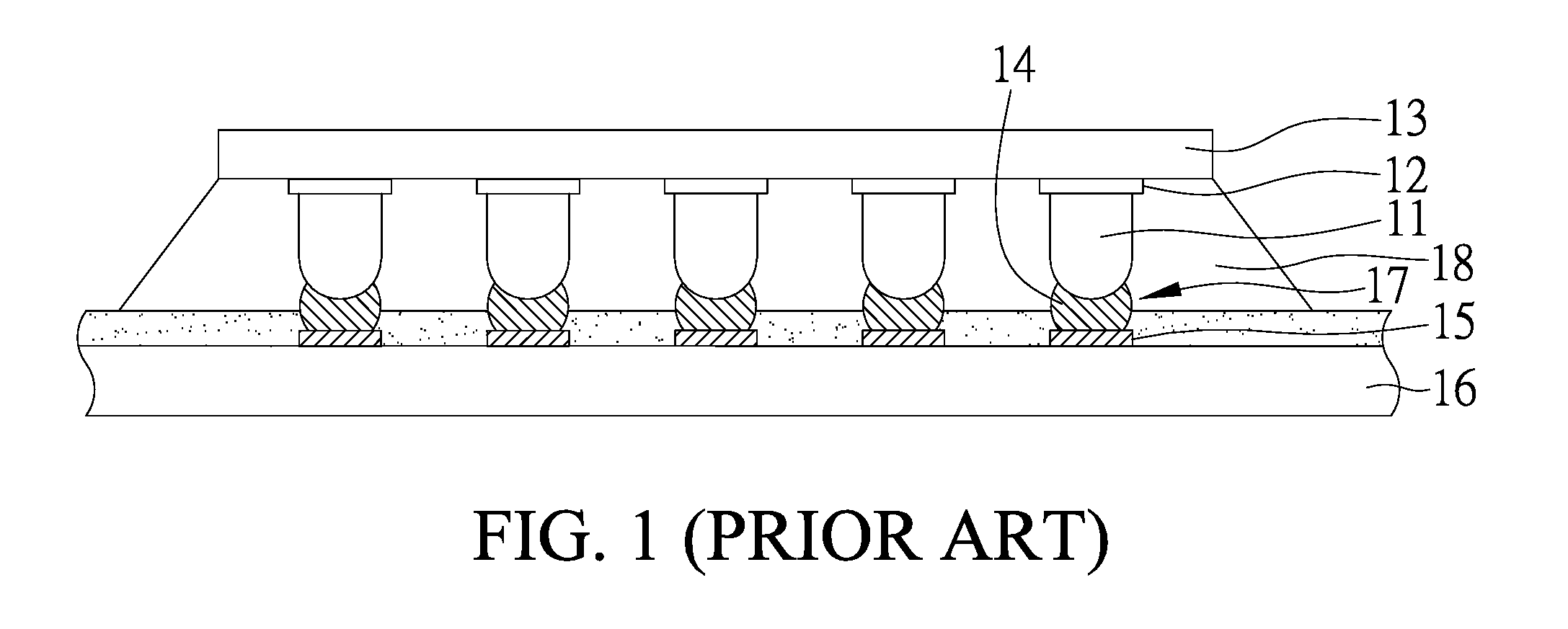
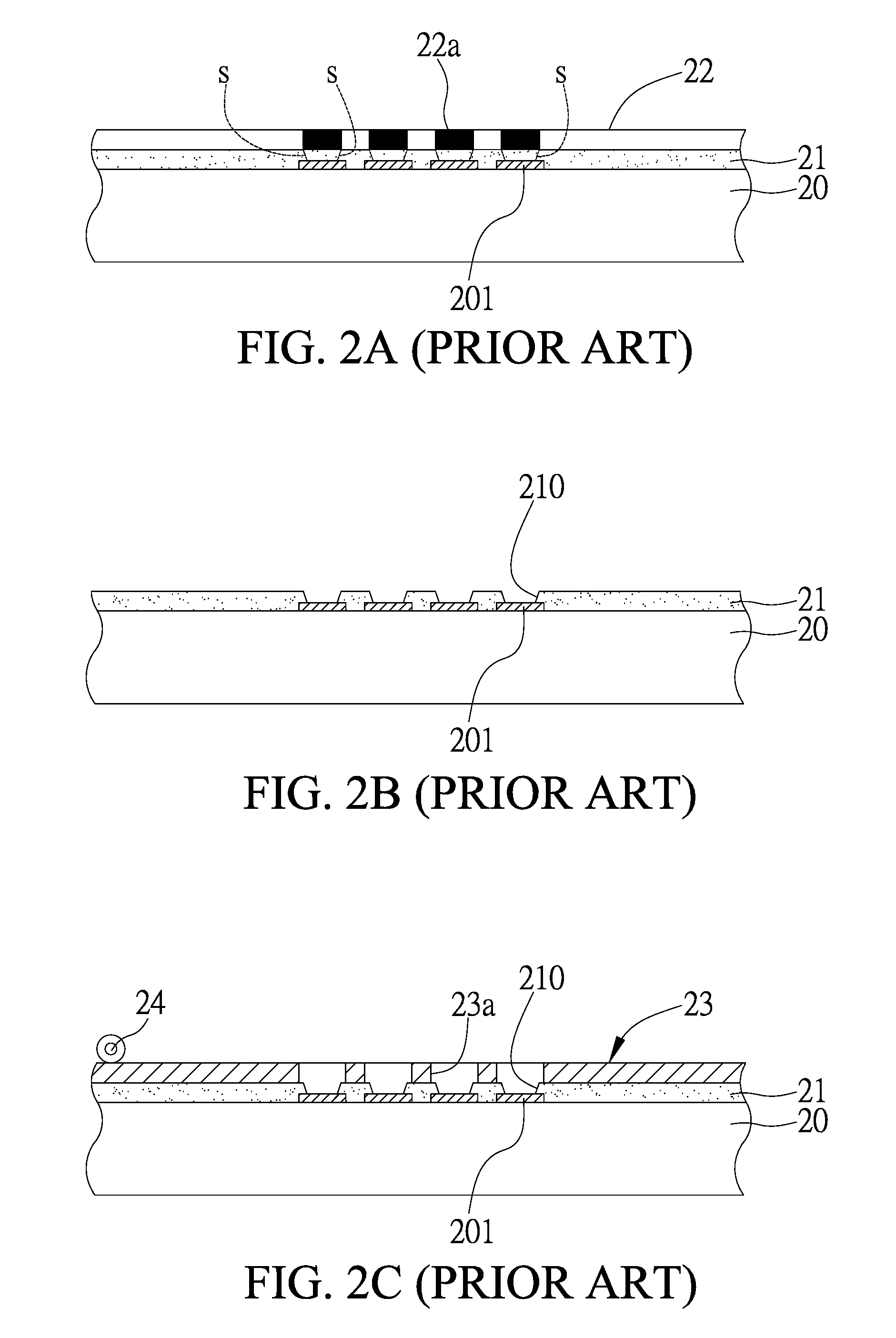
Problems solved by technology

Thus, the solder structures cannot be easily formed on the surfaces of the electrically connecting pads, and

Method used


Image

  • Circuit board surface structure and fabrication method thereof
  • Circuit board surface structure and fabrication method thereof
  • Circuit board surface structure and fabrication method thereof

Examples


Embodiment Construction

[0026]The following illustrative embodiments are provided to illustrate the disclosure of the present invention, these and other advantages and effects can be apparent to those skilled in the art after reading the disclosure of this specification.

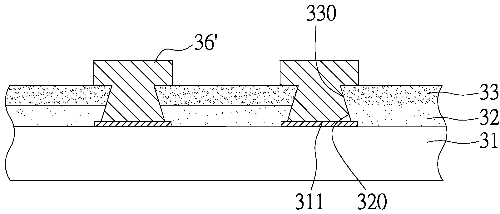
[0027]A main characteristic of the present invention is a first and a second insulating protective layers having different composition ratios are formed on a surface of a circuit board so as to facilitate forming of first and second openings having different diameters in the first and second insulating protective layers. Thus, conductive elements can be formed in the first and second openings by electroplating or stencil printing and firmly bonded in the first and second openings.

[0028]FIGS. 3A to 3H are cross-sectional views showing a fabrication method of a circuit board surface structure according to a preferred embodiment of the present invention.

[0029]Referring to FIG. 3A, a circuit board 31 that has undergone a circuit patterning proc...


PUM

PropertyMeasurementUnit
Diameteraaaaaaaaaa
Ratioaaaaaaaaaa
Electrical conductoraaaaaaaaaa

Abstract

A circuit board surface structure and a fabrication method thereof are proposed. The circuit board surface structure includes: a circuit board having a plurality of electrically connecting pads formed on at least one surface thereof; a first and a second insulating protective layers formed on the surface of the circuit board in sequence; first and a second openings respectively formed in the first and second insulating protective layers to expose the electrically connecting pads on the surface of the circuit board, wherein the first and second openings have narrow top and wide bottom and the diameter of the first openings is bigger than that of the second openings; and conductive elements formed in the first and second openings on surfaces of the electrically connecting pads. The present structure facilitates to strengthen the bonding between the conductive elements and the corresponding electrically connecting pads.

Description

BACKGROUND OF THE INVENTION[0001]1. Field of the Invention[0002]The present invention relates generally to a circuit board surface structure and fabrication method thereof, and more particularly to a method of forming conductive elements on electrically connecting pads on a circuit board surface structure for electrically connecting with an external device.[0003]2. Description of Related Art[0004]According to flip-chip technology nowadays, an IC semiconductor chip has electrode pads disposed on an active surface thereof, an organic circuit board has electrically connecting pads corresponding to the electrode pads. A solder structure or other conductive adhesive material is formed between the electrode pads of the semiconductor chip and the electrically connecting pads of the circuit board for providing electrical and mechanical connection between the semiconductor chip and the circuit board.[0005]As shown in FIG. 1, flip-chip technology involves forming a plurality of metal bumps 11...

Claims


Application Information

Patent Timeline
IPC IPC(8): H05K1/09H05K1/11H05K3/00
CPCH01L23/49811H01L2224/13017H01L2224/13018H05K3/243H05K3/3452H05K3/3473Y10T29/49124H05K3/4007H05K2201/0367H05K2201/09436H05K2203/054H05K2203/0577H05K2203/0594H05K3/3484H01L2224/05022H01L2224/05001H01L2224/05572H01L2224/05111H01L2224/05147H01L2224/05155H01L2224/05166H01L2224/05171H01L2224/05611H01L2224/05647H01L2224/05655H01L2224/05666H01L2224/05671H01L24/13H05K3/3485H01L2924/00012H01L2924/00014H01L2924/01024
Inventor TANG, SAO-HSIAWANG, YING-TUNG
Owner UNIMICRON TECH CORP
Why Eureka
Try Eureka