Multilayer printed circuit board and method of manufacturing same

a printed circuit board and multi-layer technology, applied in the direction of printed element electric connection formation, association of printed circuit non-printed electric components, conductive pattern formation, etc., can solve the problem of high impedance, difficult to make a pitch among vias in the core layer sufficiently short, and measure is not satisfactory enough to contribute to high-density wiring, etc. problem, to achieve the effect of suppressing high impedan

Inactive Publication Date: 2008-09-11
NEC CORP
View PDF0 Cites 17 Cited by
  • Summary
  • Abstract
  • Description
  • Claims
  • Application Information

AI Technical Summary

Benefits of technology

[0035]With the above configurations, the plurality of first conducting portions is formed on the board so that the edge conducting portions being adjacent to one another come near to or come into contact with one another within at least a specified distance. The center portions in regions having a plurality of first conducting portions are punched so that the partial portions on the side of center portions of the first conducting portions are removed and the edge conducting portions being adjacent to one another are at least separated from one another and, as a result, the first through-holes are formed to achieve the first conducting paths and are filled with the insulator and, then, the second through-holes each having a diameter in cross section being smaller than that of each of the first through-holes are formed inside the first through-holes filled with the insulator to realize the second conducting paths. Therefore, the interval between the first and second conducting portions can be made small and high impedance can be suppressed in transmission of high-frequency signals.

Problems solved by technology

Moreover, in the transmission of high-frequency signals in particular, since each of a signal line, power source line, or ground line is assigned at every pitch among the core layer vias 109, when a signal passes through each of the core layer vias 109, a distance of a path for a ground-return current is made long, as a result, causing high impedance.
The above conventional technologies have a problem in that it is difficult to make a pitch among vias in the core layer sufficiently short.
That is, in the above conventional technology, even if each of the core layer vias is so configured as to have a coaxial structure and the pitches among the vias are made short, the measure is not satisfactory enough to be contributable to high-density wiring.
Also, even if an outer layer of the coaxial structure is divided into two portions, it is difficult to make the pitches sufficiently short and formation of the via of this type having the coaxial structure is not easy.
Thus, both the suppression of high impedance during the transmission of high-frequency signals and the achievement of sufficiently short pitches among the vias in the conventional core layer are difficult.

Method used


Image

  • Multilayer printed circuit board and method of manufacturing same
  • Multilayer printed circuit board and method of manufacturing same
  • Multilayer printed circuit board and method of manufacturing same

Examples


first exemplary embodiment

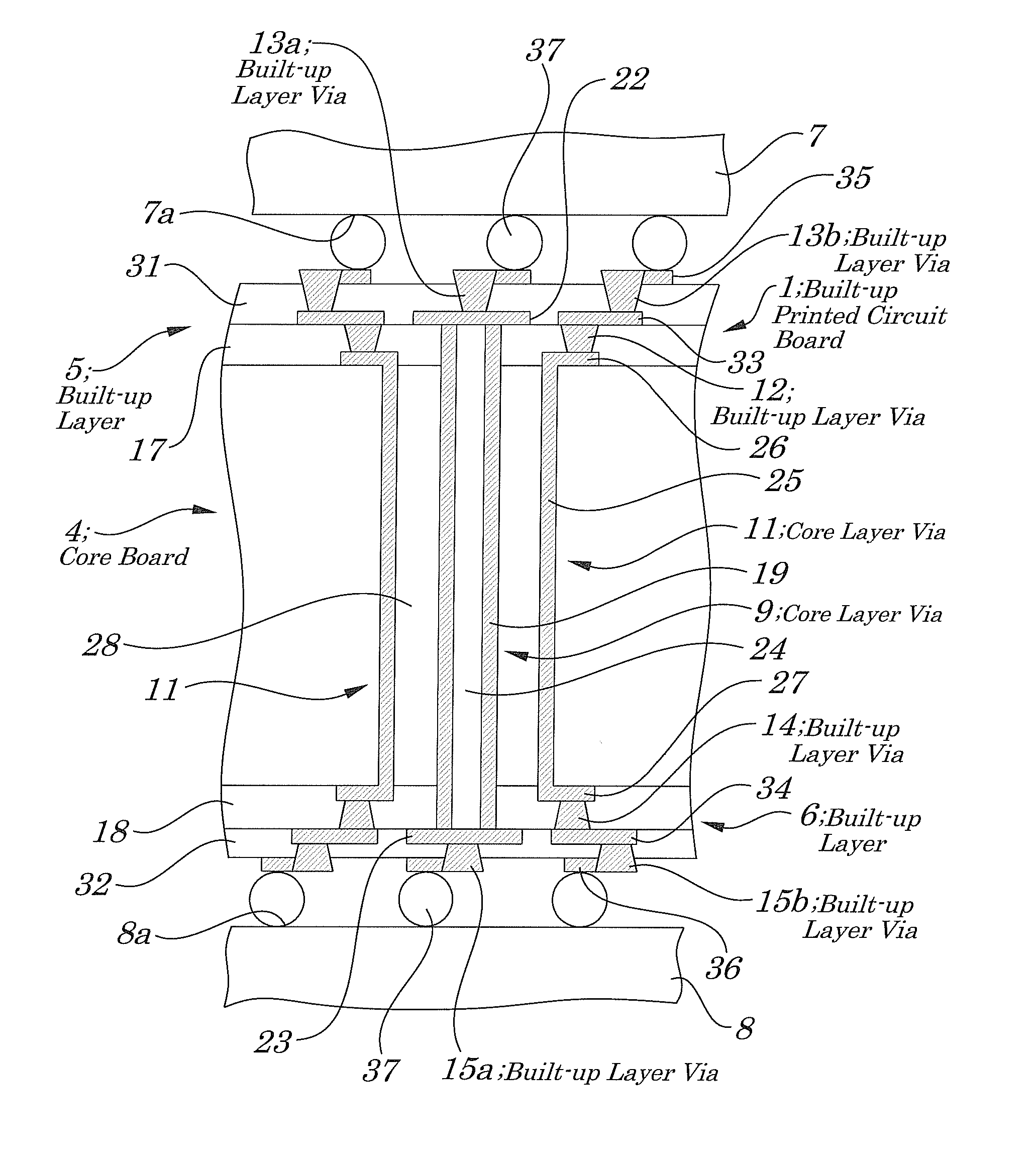
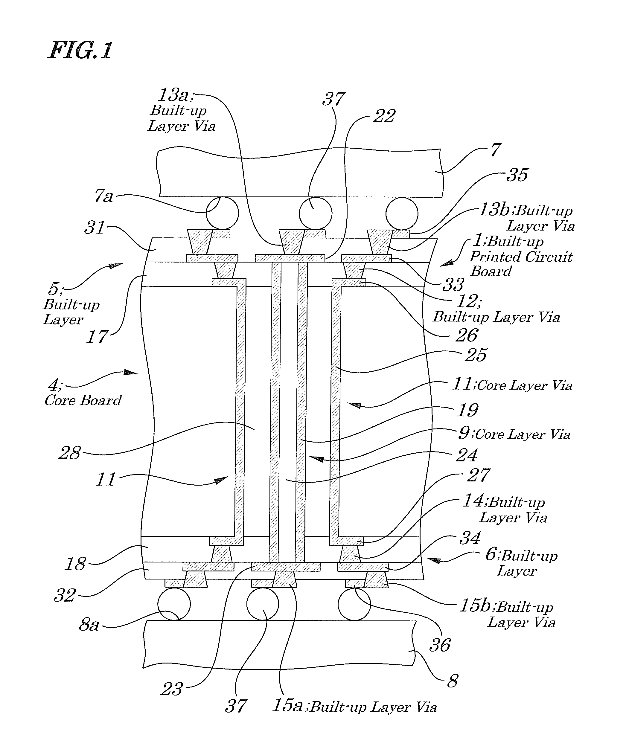
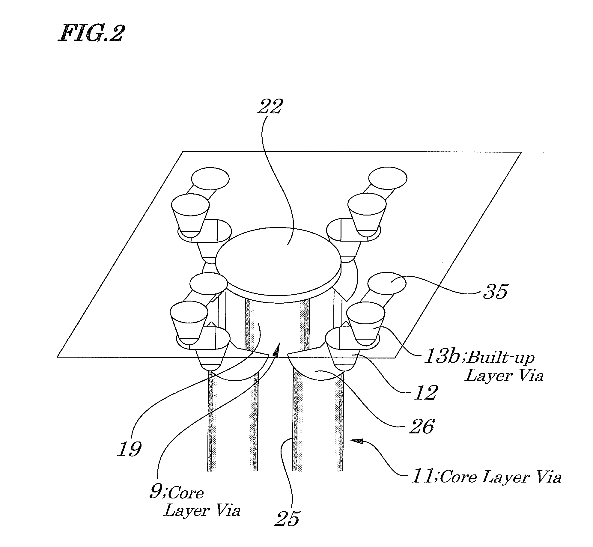
[0057]FIG. 1 is a cross-sectional view showing configurations of a built-up printed circuit board of the first exemplary embodiment of the present invention. FIG. 2 is a perspective view explaining configurations of the built-up printed circuit board of FIG. 1. FIGS. 3A to 6 are process diagrams showing a method for manufacturing the built-up printed circuit board of FIG. 1. FIGS. 7 to 12 are explanatory diagrams showing the method for manufacturing the built-up printed circuit board of FIG. 1.

[0058]The built-up printed circuit board 1 serving as a multilayer printed circuit board of the first exemplary embodiment is implemented in electronic devices such as computers and communicating devices and includes, as shown in FIGS. 1 and 2, a core board 4 having a multilayer structure in which a plurality of conducting layers and a plurality of insulating layers are stacked and built-up layers 5 and 6 formed respectively on an upper side (front side) and a lower side (rear side) of the cor...

second exemplary embodiment

[0079]FIGS. 13 to 16 are explanatory diagrams showing the method for manufacturing a built-up printed circuit board of the second exemplary embodiment of the present invention. Configurations of the built-up printed circuit board of the second exemplary embodiment differ greatly from the configurations of the first exemplary embodiment in that conducting portions (via lands) of core layer vias are overlapped. Configurations other than above are the same as those of the first exemplary embodiment and their descriptions are simplified.

[0080]In the method for manufacturing the built-up printed circuit board of the second exemplary embodiment, as shown in FIGS. 13 and 14, four core layer vias 81, 81, . . . are formed on a core board having a multilayer structure in which a plurality of conducting layers and a plurality of insulating layers are stacked. In each of the core layer vias 81, a conducting layer 83 made up of a metal plating layer being circular-arc shaped in cross section pas...

third exemplary embodiment

[0083]FIGS. 17 and 18 are an explanatory diagram showing a method for manufacturing a built-up printed circuit board of the third exemplary embodiment of the present invention. Configurations of the built-up printed circuit board of the third exemplary embodiment differ from those of the second exemplary embodiment in that six core layer vias are arranged in an overlapped manner. Configurations other than above are the same as those of the second exemplary embodiment and their descriptions are omitted accordingly.

[0084]In the method of manufacturing the built-up printed circuit board of the third exemplary embodiment, first, as shown in FIG. 17, on the core board having a multilayer structure in which a plurality of conducting layers and a plurality of insulating layers are stacked are formed six core layer vias 91, 91, . . . so that conducting portions 92 and 92 are overlapped. Each of the core layer vias 91 has a conducting layer 93 made up of a metal plated layer being cylindrica...


PUM

PropertyMeasurementUnit
thicknessaaaaaaaaaa
diameteraaaaaaaaaa
diameteraaaaaaaaaa

Abstract

A printed circuit board is provided which is capable of shortening intervals among core layer vias and suppressing high impedance. After the core layer vias each having a cylindrical conducting layer are formed so that conducting portions come into contact with one another, a punching process is performed along a symmetric axis of each of four core layer vias so that a through-hole of a specified diameter passes through a core board to form the core layer vias separated from one another and the through-hole is filled with an insulator and a punching process is performed along a central axis of the through-hole filled with the insulator so as to pass through the core board to form the through-hole having a diameter being shorter than that of the through-hole and the conducting layer is formed on an inside wall of the through-hole to form the core layer via.

Description

INCORPORATION BY REFERENCE[0001]This application is based upon and claims the benefit of priority from Japanese Patent Application No. 2007-057926, filed on Mar. 7, 2007, the disclosure of which is incorporated herein in its entirely by reference.BACKGROUND OF THE INVENTION[0002]1. Field of the Invention[0003]The present invention relates to a multilayer printed circuit board and a method for manufacturing the same, and more especially the multilayer printed circuit board such as a built-up printed circuit board and the method for manufacturing the same.[0004]2. Description of the Related Art[0005]Conventionally, an electronic device such as a computer device and communicating device generally includes a printed circuit board on which components such as SMDs (Surface Mount Devices) and through-hole mount devices are mounted.[0006]In recent years, as electronic devices become highly functional, multilayer printed circuit boards are becoming more commonly used. For example, a built-up...

Claims


Application Information

Patent Timeline
Patent Type & Authority Applications(United States)
IPC IPC(8): H05K1/18H05K3/30H05K3/42H05K3/10
CPCH05K1/0222H05K1/112H05K1/115H05K3/0047H05K3/429Y10T29/4913H05K2201/09536H05K2201/09645H05K2201/09809Y10T29/49165H05K3/4602H01L2224/16225H01L2924/15174H01L2924/15184H01L2924/15311
Inventor TAKEDA, TSUTOMU
Owner NEC CORP
Why Eureka
Try Eureka