Light emitting device, display device and a method of manufacturing display device

a technology of light emitting devices and display devices, which is applied in the manufacture of electric discharge tubes/lamps, lighting and heating apparatuses, instruments, etc., can solve the problems of large power consumption loss or the like, and achieve the effects of enhancing luminance, enhancing light distribution components, and low power consumption

Active Publication Date: 2008-09-11
SONY CORP
View PDF5 Cites 16 Cited by
  • Summary
  • Abstract
  • Description
  • Claims
  • Application Information

AI Technical Summary

Benefits of technology

[0014]However, when, for example, a use application as the display device is envisaged, such a case that its screen is visually observed at a high angle having a view angle of 70° or more is rare. Therefore, even when the characteristics of light distribution to the high angle region is enhanced more than needs, it is not said that so large merit is obtained from a viewpoint as well of realization or the like of low power consumption promotion. That is to say, further enhancing the luminance in the range of an effective visual sense than in the region of the high angle is desirable in terms of effective utilization of the emitted light from the light emitting element.
[0015]In the light of the foregoing, it is therefore desirable to provide a light emitting device having a reflecting mirror shape with which luminance within the range of an effective visual sense is remarkably enhanced by controlling a light distribution angle, distribution, etc. while uniformness of light distribution characteristics is maintained, thereby allowing high luminance promotion, low power consumption promotion, and the like, a display device, and a method of manufacturing the display device.
[0019]In the light emitting device and the display device which are constituted in the manner as described above, and a method of manufacturing the same which is constituted to have the procedure as described above, the central axis of the rotation of the parabola constituting the light reflecting surface of the concave mirror portion is set in the position of passing through the side of the parabola with respect to the middle point of the line segment joining the part of the parabola and the focal point of the parabola. Here, a light passing through the vicinity of the focal point of the parabola corresponding to a light distribution component in the high angle region when being emitted after reflection by the light reflecting surface of the concave mirror portion. Therefore, when the central axis of the rotation of the parabola is set in the position of passing through the side of the parabola, the light component passing through the vicinity of the focal point of the parabola, that is, the light distribution component in the high angle region is suppressed by an amount of approach to the side of the parabola. As a result, the light distribution component on the low angle side relatively increases.
[0020]According to the embodiments of the present invention, the light distribution component in the high angle region is suppressed by the amount of approach of the central axis of the rotation of the parabola to the side of the parabola, thereby making it possible to relatively increase the light distribution component on the side of the low angle region. This fact means that the light distribution angle, distribution, etc. can be controlled depending on the set position of the central axis of the rotation of the parabola. Therefore, according to the embodiments of the present invention, the light distribution angle, distribution, etc. are controlled while the uniformness of the light distribution characteristics is maintained, thereby making it possible to more greatly enhance the luminance within the range of the effective visual sense than that in related art one. That is to say, the bright lighting, image display, etc. can be realized with the low power consumption through the improvement in the luminance view angle characteristics due to the uniformness of the light distribution of the reflected light.

Problems solved by technology

The reason for this is because the low light extraction efficiency leads to that an amount of actual luminance in the light emitting element is not effectively utilized, which triggers a large loss in terms of power consumption or the like.

Method used


Image

  • Light emitting device, display device and a method of manufacturing display device
  • Light emitting device, display device and a method of manufacturing display device
  • Light emitting device, display device and a method of manufacturing display device

Examples


Embodiment Construction

[0036]Hereinafter, preferred embodiments of a light emitting device, a display device and a method of manufacturing the same according to the present invention will be described in detail with reference to the accompanying drawings.

[Schematic Structure of Display Device]

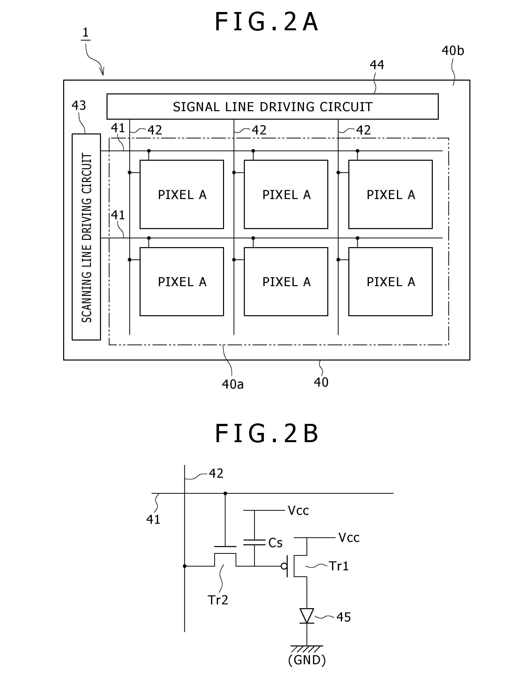
[0037]Firstly, a schematic structure of the display device will now be described. In this case, a description will be given below by giving an active matrix display device using an organic EL element as a light emitting element (hereinafter referred to as “an organic EL display”) as an example.

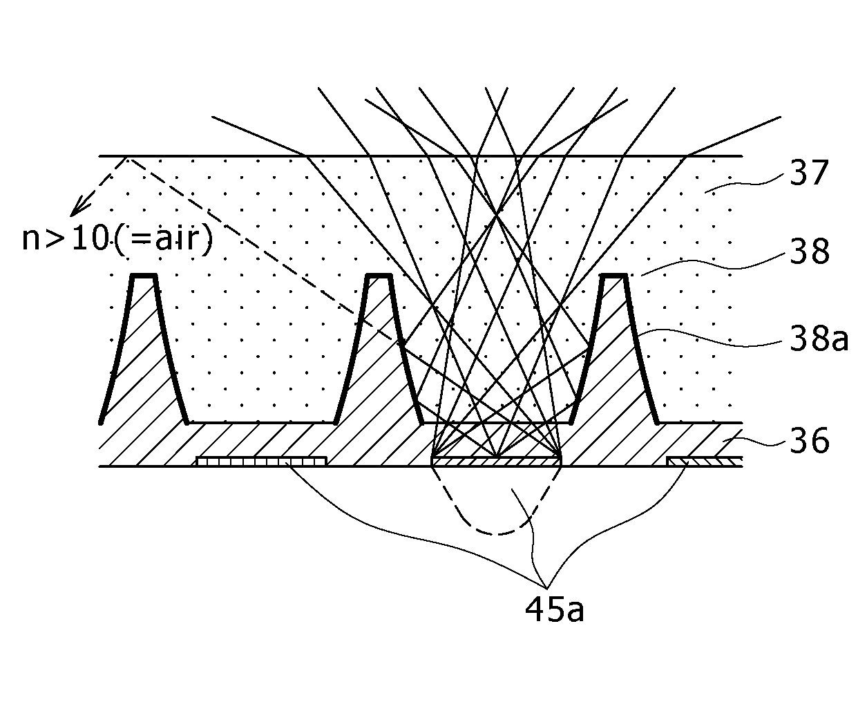
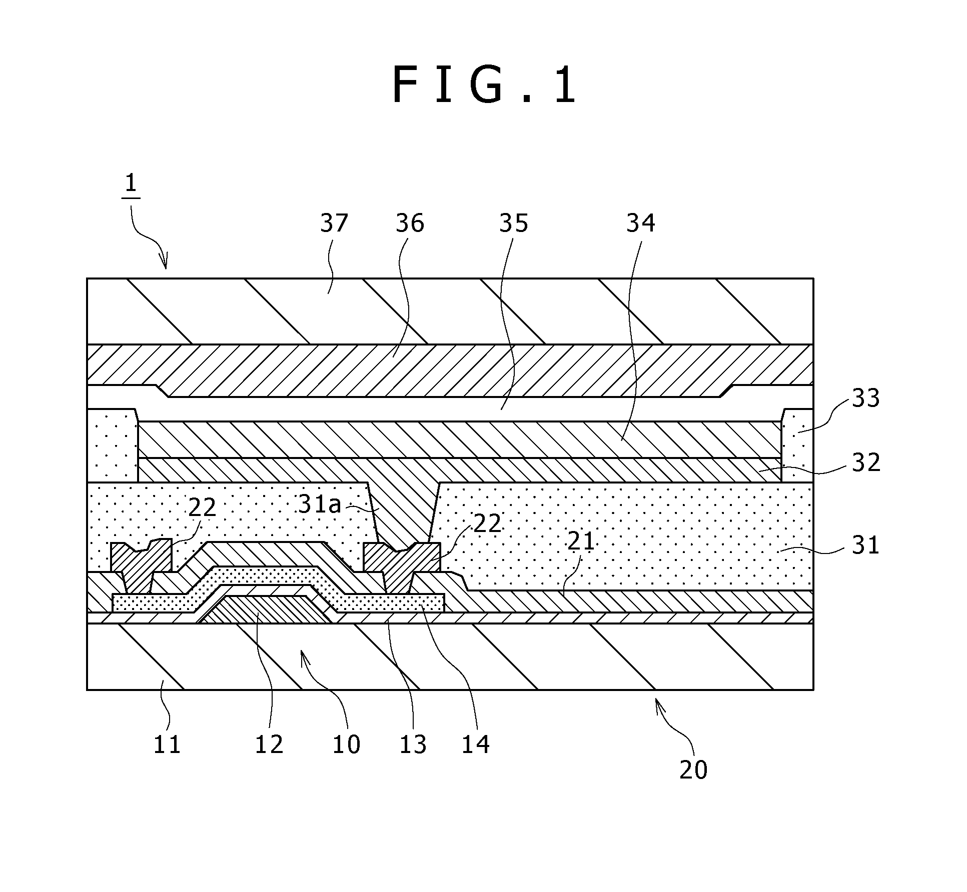
[0038]FIG. 1 is an explanatory cross sectional view showing a schematic structural example of the organic EL display.

[0039]The organic EL display 1 having a structure shown in the figure is manufactured in accordance with a procedure as will be described below.

[0040]Firstly, after a gate film 12, for example, made from a molybdenum (Mo) film is formed through patterning on a substrate 11 made from a glass substrate, the entire ...


PUM


Abstract

Disclosed herein is a light emitting device, which includes a light emitting element configured to emit a light, and a concave mirror portion configured to reflect the light emitted from the light emitting element, the concave mirror portion being erected on a circumference of an emission surface of the light emitting element. The concave mirror portion has a light reflecting surface obtained by rotating a part of a parabola. A central axis of the rotation is set in a position of passing through a side of the parabola with respect to a middle point of a line segment joining the part of the parabola and a focal point of the parabola.

Description

CROSS REFERENCES TO RELATED APPLICATIONS[0001]The present invention contains subject matter related to Japanese Patent Application JP 2007-056598 filed in the Japanese Patent Office on Mar. 7, 2007, the entire contents of which being incorporated herein by reference.BACKGROUND OF THE INVENTION[0002]1. Field of the Invention[0003]The present invention relates to a light emitting device, a display device and a method of manufacturing the display device.[0004]2. Description of the Related Art[0005]In recent years, light emitting devices (hereinafter referred to as “LEDs” for short), and organic light emitting diodes (hereinafter referred to as “OLEDs” for short) have been in widespread use as light emitting elements. Also, the LEDs and the OLEDs are widely utilized in the various fields of a light emitting device constituting lighting equipment, a display device called a flat panel display, and the like.[0006]In the case where the light emitting device, the display device or the like i...

Claims


Application Information

Patent Timeline
Patent Type & Authority Applications(United States)
IPC IPC(8): F21V7/06H01J9/00
CPCY10S362/80H01L51/5271H10K50/856G02F1/1335
Inventor FUKUDA, TOSHIHIROYAMADA, JIROASAI, NOBUTOSHI
Owner SONY CORP
Why Eureka
Try Eureka