Substrate processing apparatus, substrate processing method and storage medium

a substrate processing and substrate technology, applied in the direction of chemistry apparatus and processes, cleaning processes and apparatus, cleaning, etc., can solve the problems of contamination of wafers, increased footprint, contamination of wafers, etc., and achieve the effect of rapid heating and cooling of substrates

Inactive Publication Date: 2008-09-18
TOKYO ELECTRON LTD
View PDF3 Cites 9 Cited by
  • Summary
  • Abstract
  • Description
  • Claims
  • Application Information

AI Technical Summary

Benefits of technology

[0011]According to the present invention, the state in which the substrate is placed on the mounting table and processed in the process chamber while being temperature-adjusted by the first temperature adjusting mechanism and the state in which the substrate is lifted up from the mounting table and processed in the process chamber while being temperature-adjuste

Problems solved by technology

However, such a processing apparatus in which the chemical processing chamber and the heat treatment chamber are separately provided has a disadvantage that the apparatus becomes large, leading to an increase in footprint since the number of process chambers increases.
Further, separately provi

Method used


Image

  • Substrate processing apparatus, substrate processing method and storage medium
  • Substrate processing apparatus, substrate processing method and storage medium
  • Substrate processing apparatus, substrate processing method and storage medium

Examples


Embodiment Construction

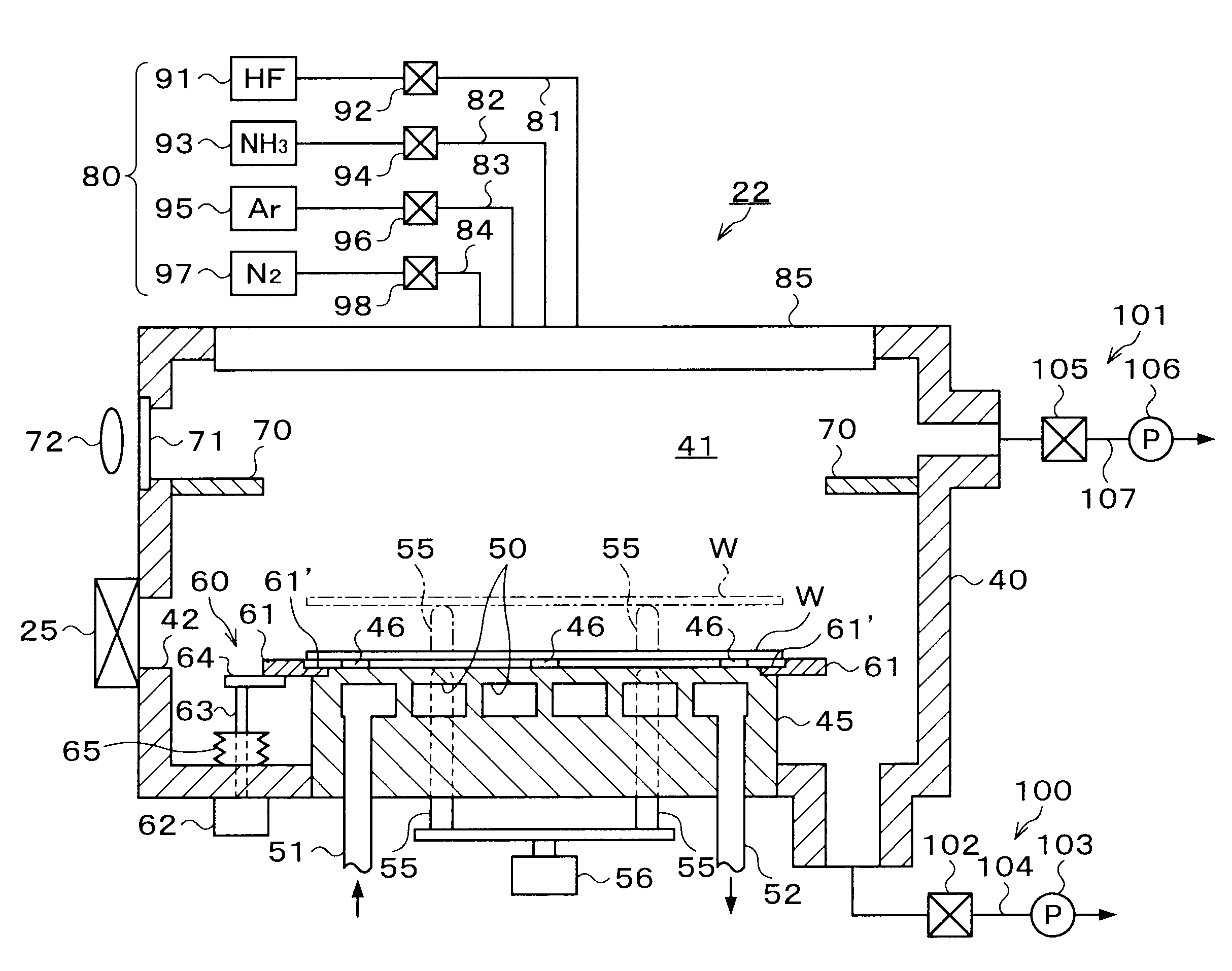
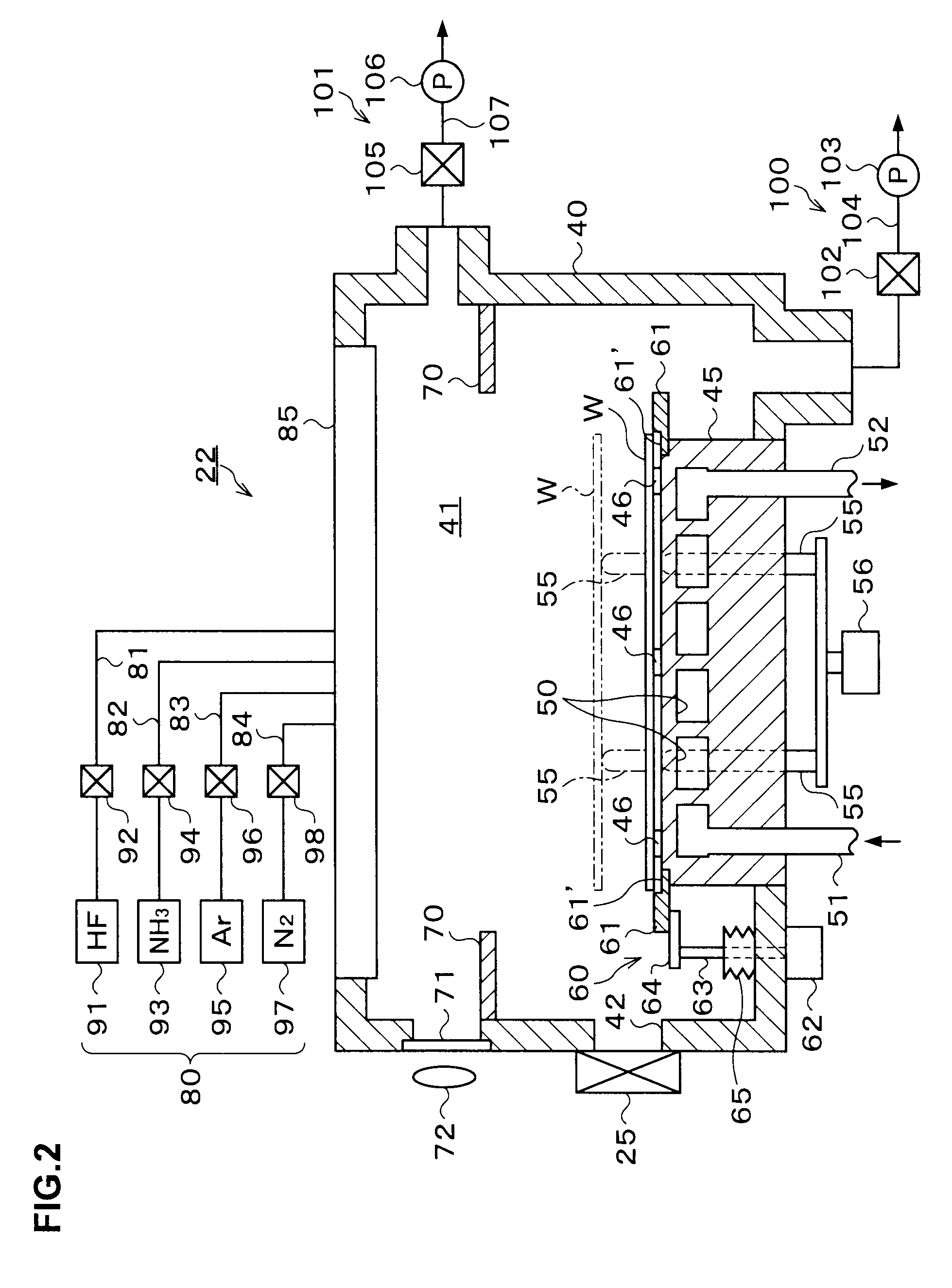
[0019]Hereinafter, an embodiment of the present invention will be described in which an oxide film (silicon dioxide (SiO2)) formed on a surface of a semiconductor wafer (hereinafter, referred to as a “wafer”) is removed by COR processing as an example of substrate processing. In the specification and drawings, constituent elements having substantially the same functions and structures are denoted by the same reference numerals and symbols, and redundant description thereof will be omitted.

(Overall Description of Processing System)

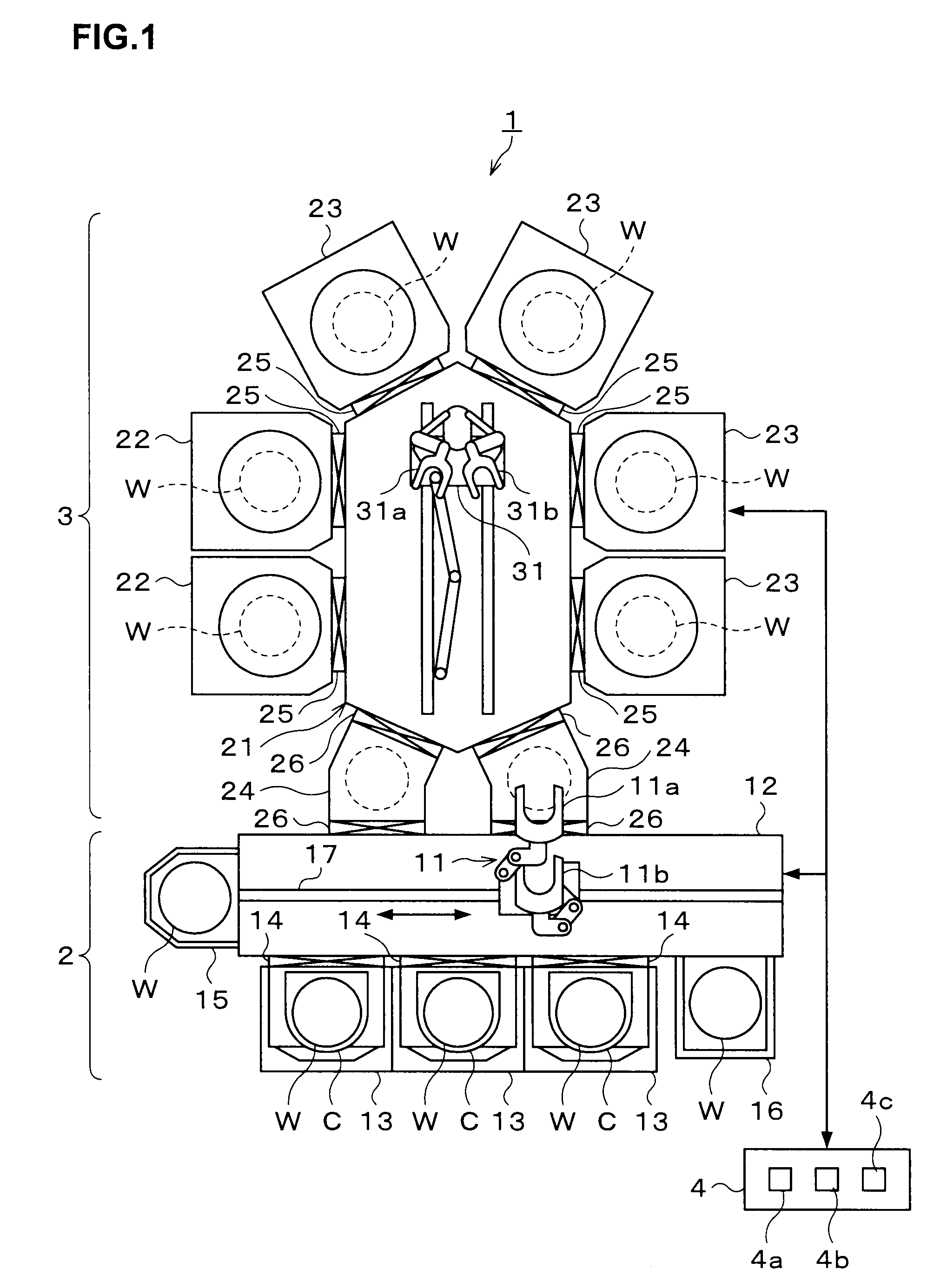
[0020]FIG. 1 is a plane view showing a rough configuration of a processing system 1 including COR apparatuses 22 according to the embodiment of the present invention. The processing system 1 is configured to apply COR (Chemical Oxide Removal) processing and film forming processing to a wafer W as an example of a substrate to be processed. In the COR processing, chemical processing to turn a natural oxide film on a surface of the wafer W into a reaction prod...


PUM

PropertyMeasurementUnit
Temperatureaaaaaaaaaa

Abstract

A substrate processing apparatus includes: a mounting table to have the substrate placed thereon in a process chamber; a first temperature adjusting mechanism temperature-adjusting the substrate placed on the mounting table; a lifter mechanism lifting up the substrate from the mounting table in the process chamber; and a second temperature adjusting mechanism temperature-adjusting the substrate lifted up from the mounting table by the lifter mechanism, wherein the first temperature adjusting mechanism and the second temperature adjusting mechanism temperature-adjust the substrate to different temperatures respectively.

Description

BACKGROUND OF THE INVENTION [0001]1. Field of the Invention[0002]The present invention relates to a substrate processing apparatus, a substrate processing method, and a storage medium.[0003]2. Description of the Related Art[0004]In manufacturing processes of semiconductor devices, for instance, various processing steps are performed while the inside of a process chamber housing a semiconductor wafer (hereinafter, referred to as a “wafer”) is set in a low-pressure state close to a vacuum state. As an example of the processing utilizing such a low-pressure state, there has been know COR (Chemical Oxide Removal) processing for chemically removing an oxide film (silicon dioxide (SiO2)) existing on a surface of a wafer (see, the specification of US Patent Application Publication No. 2004 / 0182417 and the specification of US Patent Application Publication No. 2004 / 0184792). In this COR processing, under the low-pressure state, mixed gas of hydrogen fluoride gas (HF) and ammonia gas (NH3) i...

Claims


Application Information

Patent Timeline
IPC IPC(8): B08B7/00H01L21/67B08B13/00H01L21/302
CPCH01L21/02057H01L21/31116H01L21/67248H01L29/7848H01L29/165H01L29/66628H01L29/66636H01L21/68742
Inventor ONISHI, TADASHI
Owner TOKYO ELECTRON LTD
Why Eureka
Try Eureka