Semiconductor Oxidation Apparatus and Method of Producing Semiconductor Element

a technology of oxidation apparatus and semiconductor element, which is applied in the direction of semiconductor/solid-state device testing/measurement, gas-gas reaction process, instruments, etc., can solve the problems of affecting the amount of oxidation of semiconductor sample b>1020/b>, yield deterioration, etc., to achieve accurate monitoring, control the amount of oxidation, and uniform characteristics

Inactive Publication Date: 2008-09-25
RICOH KK +1
View PDF2 Cites 52 Cited by
  • Summary
  • Abstract
  • Description
  • Claims
  • Application Information

AI Technical Summary

Benefits of technology

[0008]A more specific object of the present invention is to provide a semiconductor oxidation apparatus and a method of producing semiconductor element, which can maintain an amount of oxidation of a selectively oxidizing layer included in a semiconductor sample uniform in an in-plane direction, and appropriately control the amount of oxidation.
[0009]Still another object of the present invention is to provide a semiconductor oxidation apparatus comprising a sealable oxidation chamber defined by walls; a base provided within the oxidation chamber and configured to support a semiconductor sample; a supply part configured to supply water vapor into the oxidation chamber to oxidize a specific portion of the semiconductor sample; a monitoring window provided in one of the walls of the oxidation chamber and disposed at a position capable of confronting the semiconductor sample supported on the base; a monitoring part provided outside the oxidation chamber and capable of confronting the semiconductor sample supported on the base via the monitoring window; and an adjusting part configured to adjust a distance between the base and the monitoring part. According to the semiconductor oxidation apparatus of the present invention, it is possible to adjust the temperature distribution and the vapor density distribution of the semiconductor sample uniform during the oxidation process, and the oxidation rate of the semiconductor sample can be accurately monitored and evaluated at the time of the monitoring. Hence, it is possible to produce semiconductor elements having uniform characteristics.
[0012]A further object of the present invention is to provide a method of producing a semiconductor element by placing within a water vapor atmosphere a semiconductor sample that includes a mesa having a semiconductor layer including Al and As, and forming a current constricting part and a current injecting part that is surrounded by the current constricting part in the semiconductor layer by oxidizing the semiconductor layer from a peripheral end of the semiconductor layer appearing at an outer peripheral side surface of the mesa towards an inner radial direction so as to leave a central portion of the semiconductor layer non-oxidized, the method comprising the steps of (a) interrupting an oxidation process at least once during oxidation of the semiconductor layer; and (b) monitoring an oxidation rate of the semiconductor layer while the oxidation process is interrupted. According to the method of the present invention, it is possible to accurately evaluate the oxidation rate at the time when the oxidation process is interrupted, and produce semiconductor elements having uniform characteristics.

Problems solved by technology

However, the amount of oxidation of the semiconductor sample 1020 is affected by inconsistencies among the lots, such as the composition and the film thickness after the crystal growth in a semiconductor film forming apparatus.
As a result, the size of the current constricting part causes the inconsistency in the oscillation characteristic such as the optical output, and the yield deteriorates.

Method used


Image

  • Semiconductor Oxidation Apparatus and Method of Producing Semiconductor Element
  • Semiconductor Oxidation Apparatus and Method of Producing Semiconductor Element
  • Semiconductor Oxidation Apparatus and Method of Producing Semiconductor Element

Examples


first embodiment

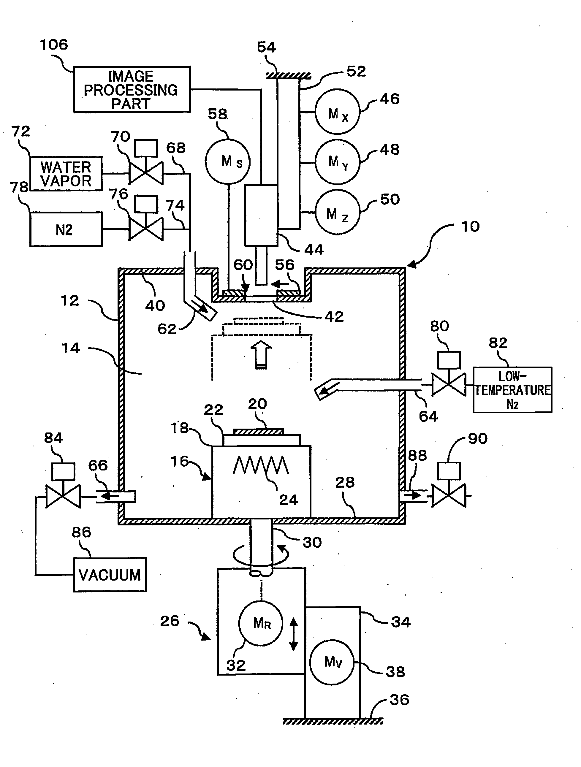
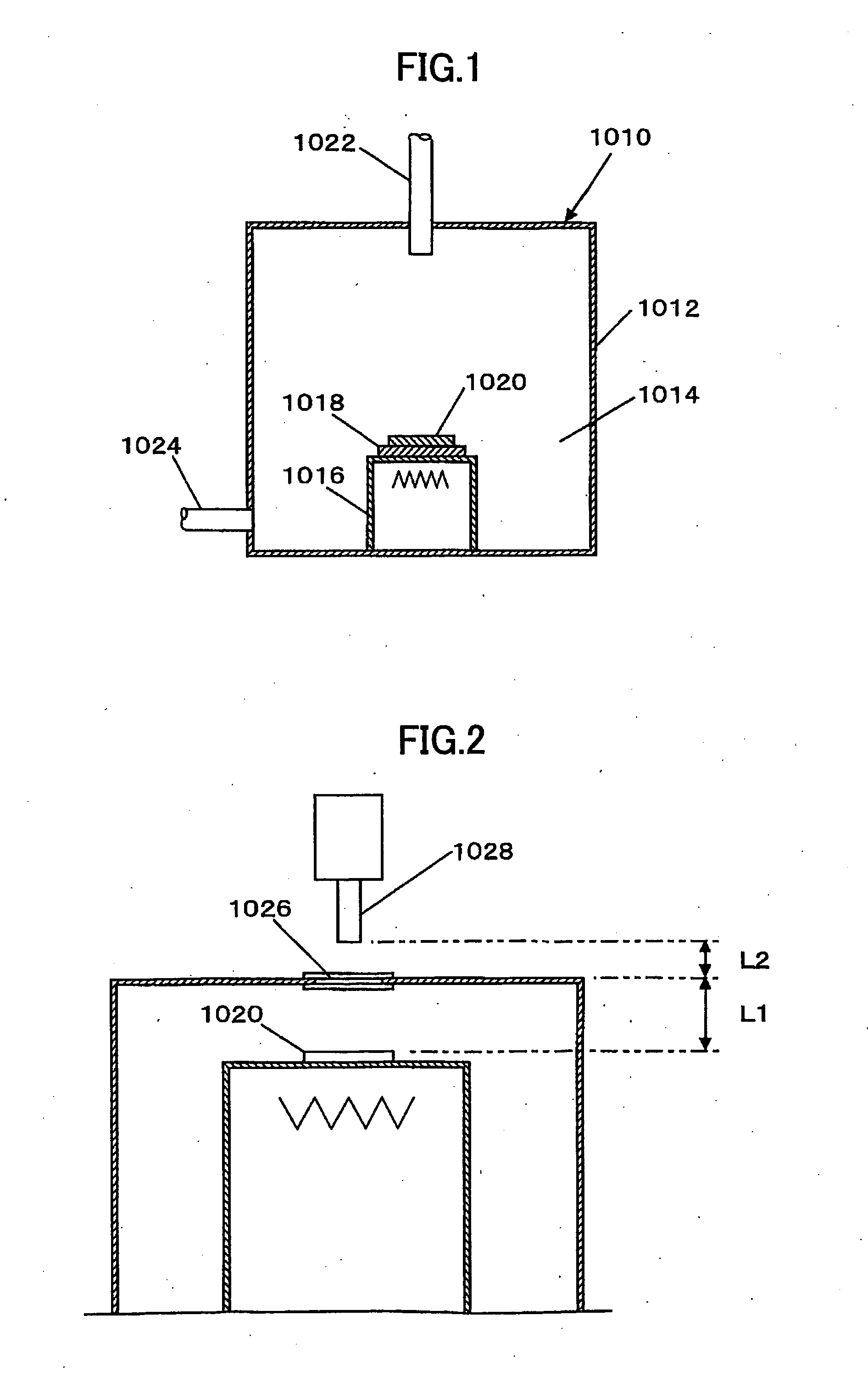
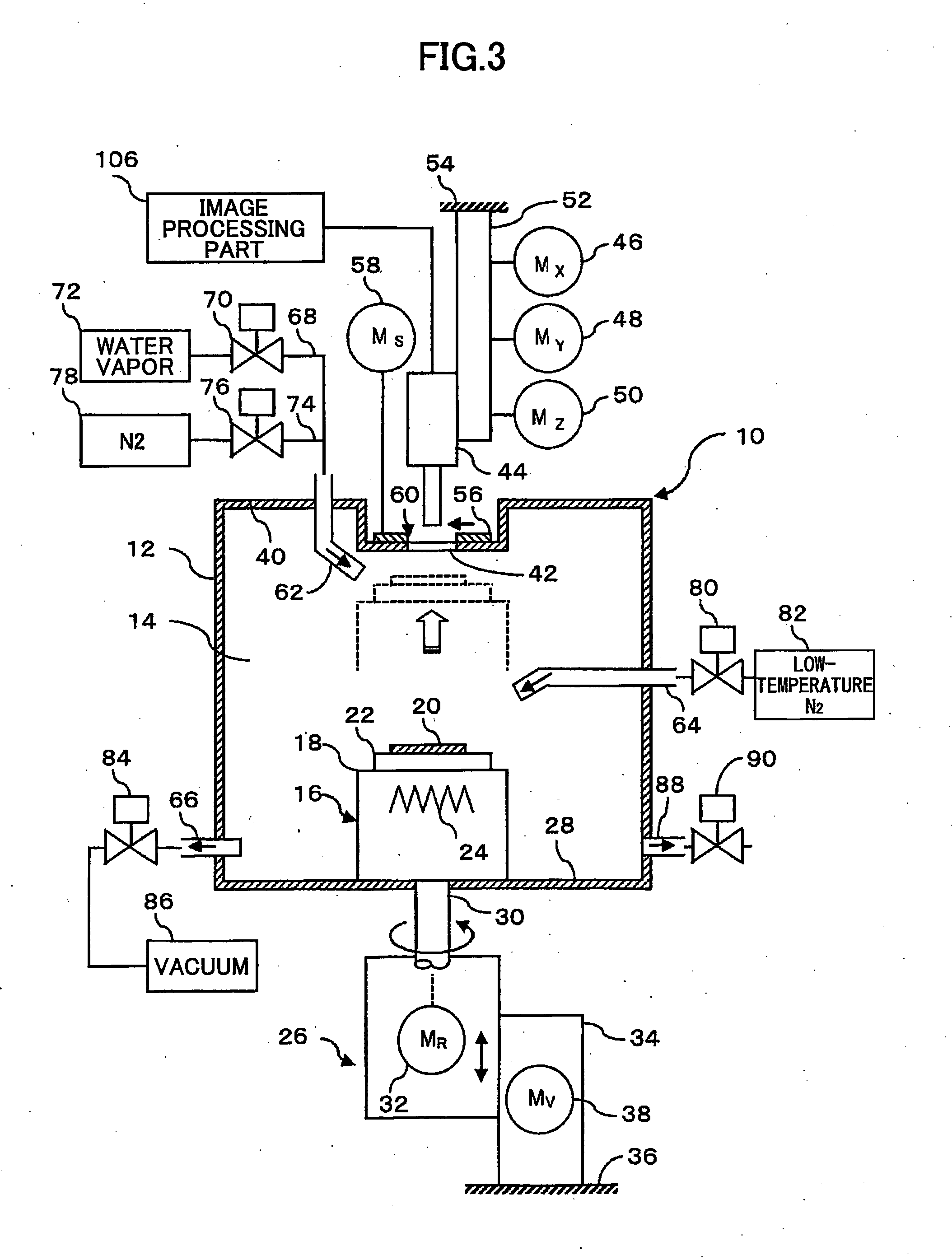
[0038]FIG. 3 is a cross sectional view showing a structure of a first embodiment of the semiconductor oxidation apparatus according to the present invention in a vertical cross section. A semiconductor oxidation apparatus (hereinafter simply referred to as an oxidation apparatus) 10 shown in FIG. 3 has a pressure-tight sealable container (or oxidation chamber) 12 made of a metal such as stainless steel. An internal space 14 having a predetermined size is provided within the oxidation chamber 12, and a base 16 for supporting a semiconductor sample is provided at the bottom of the internal space 14.

[0039]In this embodiment, the base 16 is made up of a heating table 18, and a sample table (or substrate holder) 22 that is provided on the heating table 18 and is designed to support thereon a semiconductor sample (substrate made of semiconductor wafer) 20 that is to be oxidized. The heating table 18 has an electric heater 24 for heating the semiconductor sample 20 that is to be oxidized, ...

second embodiment

[0078]FIG. 15 is a cross sectional view showing a structure of a VCSEL produced by a second embodiment of the present invention. A VCSEL 300 shown in FIG. 15 outputs a laser oscillation having a wavelength of 780 nm, and has an n-(100)GaAs substrate 302 having an inclination angle of 2° in a direction of the face orientation. An n-Al0.9Ga0.1As layer and an n-Al0.3Ga0.7As layer are alternately stacked for 35.5 periods on the substrate 302, to form a periodic structure having a thickness that is ¼ the oscillation wavelength within the medium and forming an n-semiconductor distributed Bragg reflection mirror (hereinafter referred to as a first reflection mirror or simply n-DBR mirror) 304. Between two mutually adjacent n-Al0.9Ga0.1As and n-Al0.3Ga0.7As layers, there is inserted a composition inclined layer (not shown) having a thickness of 20 nm and in which the Al composition gradually changes from the Al composition of the n-Al0.9Ga0.1As layer to the Al composition of the n-Al0.3Ga0...


PUM


Abstract

A semiconductor oxidation apparatus is provided with a sealable oxidation chamber defined by walls, a base provided within the oxidation chamber and configured to support a semiconductor sample, a supply part configured to supply water vapor into the oxidation chamber to oxidize a specific portion of the semiconductor sample, a monitoring window provided in one of the walls of the oxidation chamber and disposed at a position capable of confronting the semiconductor sample supported on the base, a monitoring part provided outside the oxidation chamber and capable of confronting the semiconductor sample supported on the base via the monitoring window, and an adjusting part configured to adjust a distance between the base and the monitoring part.

Description

TECHNICAL FIELD[0001]The present invention generally relates to semiconductor oxidation apparatuses and methods of producing semiconductor element, and more particularly to a semiconductor oxidation apparatus and a method of producing semiconductor element, which oxidize a semiconductor element including aluminum (Al) and arsenide (As) from an outer peripheral edge portion towards a central portion, and are particularly suited for producing an oxidized constricting type surface-emitting laser in which sizes of a current constricting part and a current injecting part are appropriately adjusted.BACKGROUND ART[0002]There are semiconductor lasers having a current constricting structure in order to improve the current flow efficiency. A vertical-cavity surface-emitting laser (VCSEL) is an example of such a semiconductor laser. The VCSEL emits light in a direction perpendicular to a substrate, and compared to the so-called edge-emitting semiconductor lasers, the VCSEL has low cost, low po...

Claims


Application Information

Patent Timeline
Patent Type & Authority Applications(United States)
IPC IPC(8): B01J19/00H01L21/469
CPCH01S5/18313H01S5/2215H01S5/18358
Inventor SATO, SHUNICHIJIKUTANI, NAOTOITOH, AKIHIROUMEMOTO, SHINYAZENNO, YOSHIAKIYAMAMOTO, TAKATOSHI
Owner RICOH KK
Why Eureka
Try Eureka