Plasma nitrided gate oxide, high-k metal gate based CMOS device

a technology of metal gate and plasma nitride, which is applied in the direction of semiconductor devices, electrical devices, transistors, etc., can solve the problems of increasing power dissipation and heat, affecting the work efficiency of hafnium based dielectrics, and affecting the work efficiency of semiconductor devices

Inactive Publication Date: 2008-10-02
TEXAS INSTR INC
View PDF8 Cites 139 Cited by
  • Summary
  • Abstract
  • Description
  • Claims
  • Application Information

AI Technical Summary

Benefits of technology

[0004]In accordance with the present teachings, there is a method of making a CMOS device. The method can include providing a substrate including a first active region and a second active region and forming a high-K layer over the first active region and the second active region. The method can also include forming a first dielectric capping layer disposed on the high-K layer over the first active region, forming a second dielectric capp

Problems solved by technology

With the decrease in the size of transistors, the thickness of the silicon oxide gate dielectric has become only a few atomic layers thick, resulting in tunneling current leakage and

Method used


Image

  • Plasma nitrided gate oxide, high-k metal gate based CMOS device
  • Plasma nitrided gate oxide, high-k metal gate based CMOS device
  • Plasma nitrided gate oxide, high-k metal gate based CMOS device

Examples


Embodiment Construction

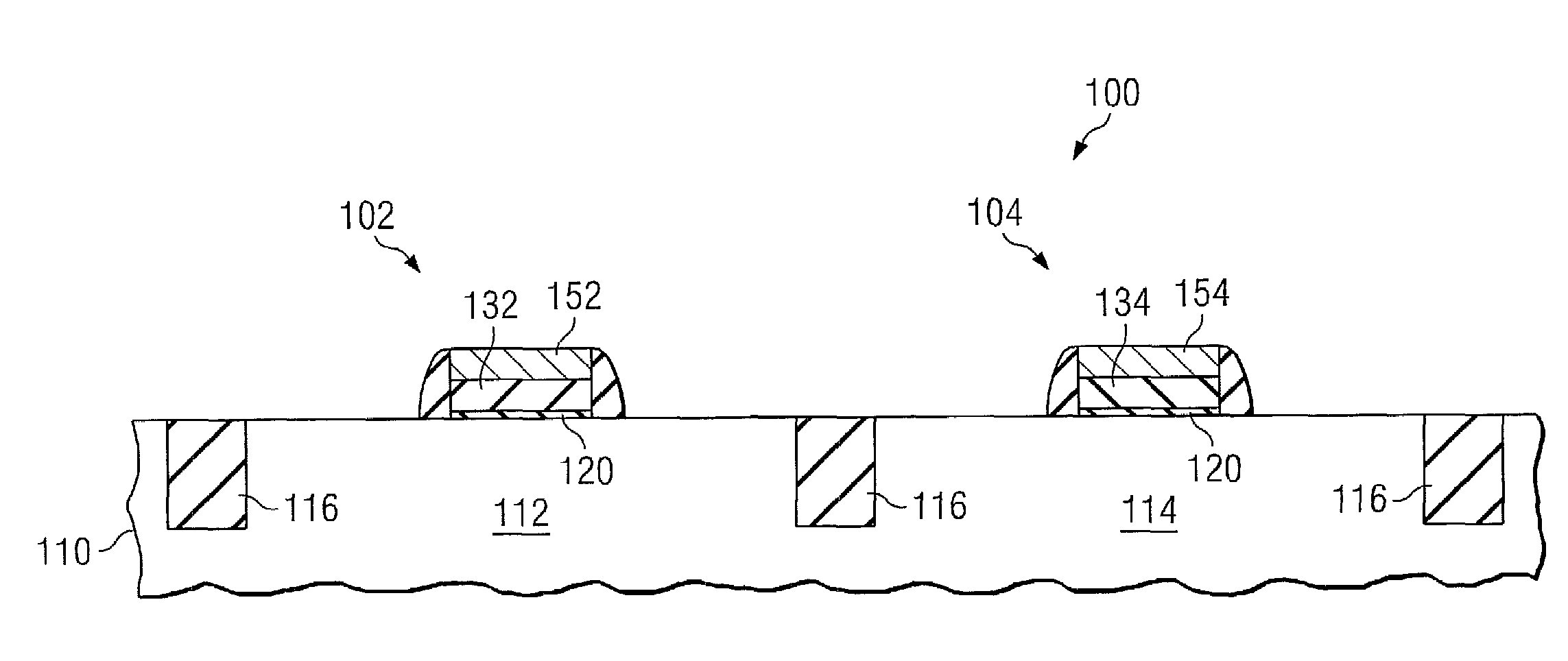
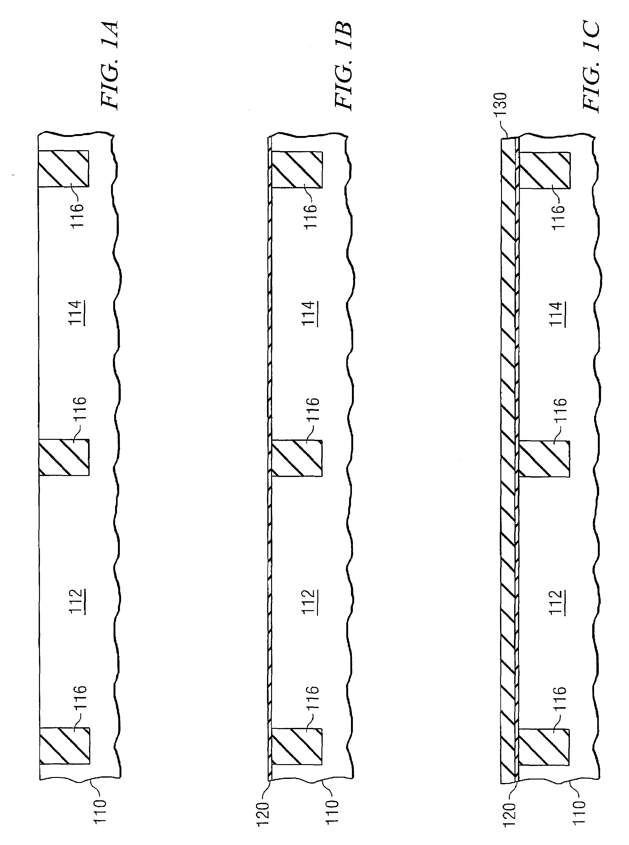
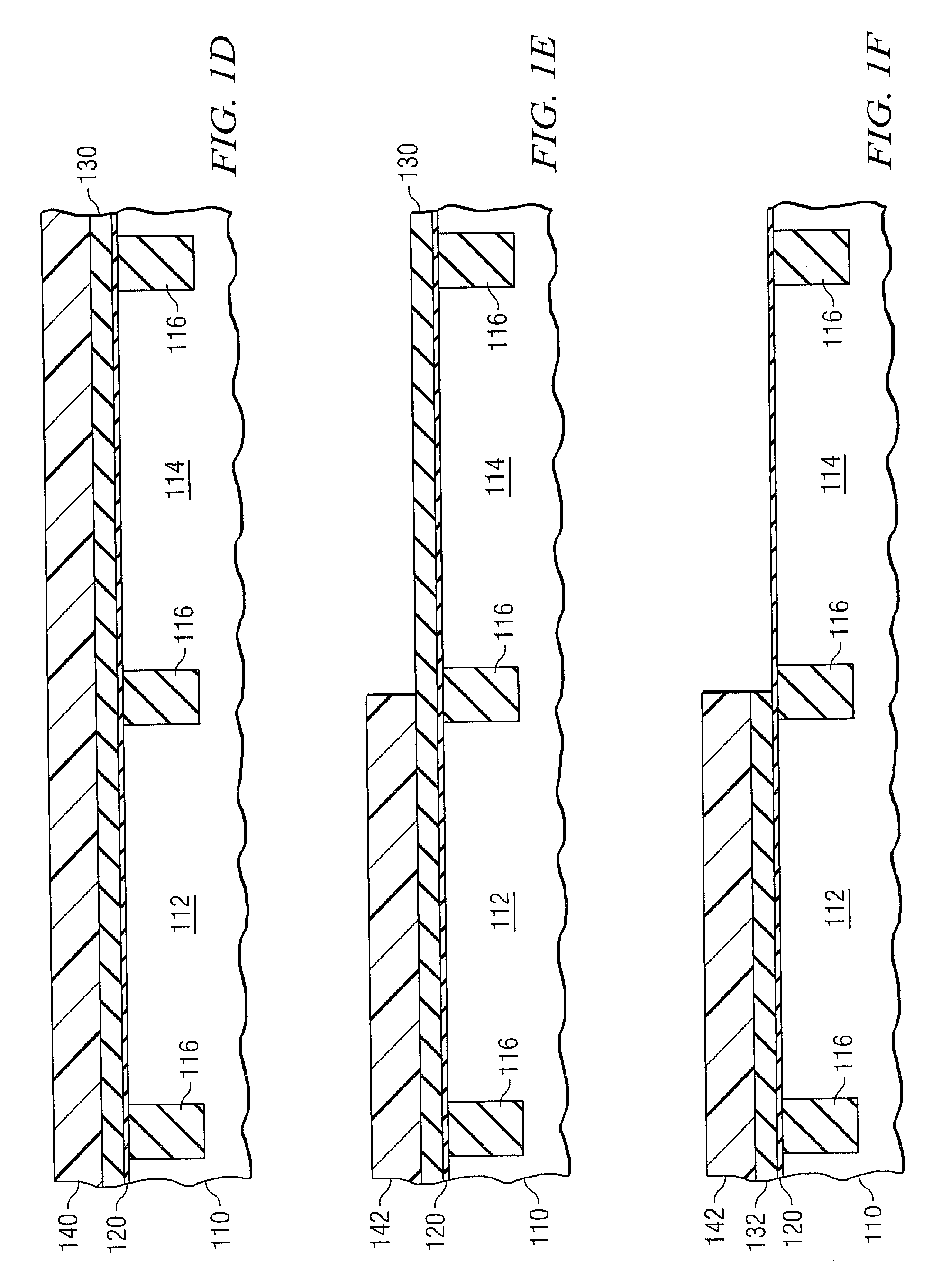
[0013]Reference will now be made in detail to the exemplary embodiments, examples of which are illustrated in the accompanying drawings. Wherever possible, the same reference numbers will be used throughout the drawings to refer to the same or like parts.

[0014]Notwithstanding that the numerical ranges and parameters setting forth the broad scope of the invention are approximations, the numerical values set forth in the specific examples are reported as precisely as possible. Any numerical value, however, inherently contains certain errors necessarily resulting from the standard deviation found in their respective testing measurements. Moreover, all ranges disclosed herein are to be understood to encompass any and all sub-ranges subsumed therein. For example, a range of “less than 10” can include any and all sub-ranges between (and including) the minimum value of zero and the maximum value of 10, that is, any and all sub-ranges having a minimum value of equal to or greater than zero ...


PUM


Abstract

In accordance with the invention, there are CMOS devices and semiconductor devices and methods of fabricating them. The CMOS device can include a substrate including a first active region and a second active region and a first transistor device over the first active region, wherein the first transistor device includes a high-K layer over the first active region, a first dielectric capping layer on the high-K layer, and a first metal gate layer over the first dielectric capping layer. The CMOS device can also include a second transistor device over the second active region, wherein the second transistor device includes a high-K layer over the second active region, a second dielectric capping layer on the second high-K layer, and a second metal gate layer over the second dielectric capping layer.

Description

FIELD OF THE INVENTION[0001]The subject matter of this invention relates to methods of fabricating semiconductor devices. More particularly, the subject matter of this invention relates to devices and methods of fabricating plasma nitrided gate oxide, high-k metal gate based devices.BACKGROUND OF THE INVENTION[0002]With the decrease in the size of transistors, the thickness of the silicon oxide gate dielectric has become only a few atomic layers thick, resulting in tunneling current leakage and an increase in the power dissipation and heat. Thus, there is a need to use high-k gate dielectrics with a lower equivalent oxide thickness (EOT) for better performance. The use of high-k gate dielectrics also requires metal gates that can replace polysilicon gates. Hafnium based gate dielectrics have demonstrated transistor characteristics and mobilities as good as those of silicon oxynitride gate dielectrics. However, it has been difficult with hafnium based dielectrics to obtain work funct...

Claims


Application Information

Patent Timeline
IPC IPC(8): H01L27/108H01L21/8238
CPCH01L21/02164H01L21/02181H01L21/02189H01L21/02332H01L21/0234H01L21/28194H01L21/28202H01L21/3145H01L21/31604H01L21/31616H01L21/31641H01L21/31645H01L21/823828H01L21/823857H01L27/092H01L29/4966H01L29/513H01L29/517H01L29/518
Inventor ALSHAREEF, HUSAM NIMANQUEVEDO-LOPEZ, MANUEL
Owner TEXAS INSTR INC
Why Eureka
Try Eureka