Semiconductor capacitor structure and layout pattern thereof

a technology of semiconductor capacitors and capacitors, which is applied in the direction of capacitors, semiconductor devices, and semiconductor/solid-state device details, etc., can solve the problems of unsatisfactory electrical characteristics, low manufacturing cost of mim capacitors, and insufficient geometrical symmetry of interdigitated metal capacitors, so as to improve the geometrical symmetry, improve the capacitance effect, and improve the effect of geometric symmetry

Inactive Publication Date: 2008-10-02
REALTEK SEMICON CORP
View PDF15 Cites 9 Cited by
  • Summary
  • Abstract
  • Description
  • Claims
  • Application Information

AI Technical Summary

Benefits of technology

[0011]It is therefore one of the objectives of the present invention to provide a semiconductor capacitor structure having a plurality of symmetrical ring type sections and an improved geometrical symmetry, and thus the semiconductor capacitor structure of the present invention can attain a better capacitance effect and have a higher unit capacitance than conventional designs.

Problems solved by technology

However, since the manufacturing cost for the MIM capacitor structure is very expensive, mainly due to the additional photomask(s) required in the manufacturing process, and as the cost becomes more significant along with development of advanced semiconductor manufacturing process technologies, an interdigitated metal capacitor of metal-oxide-metal (MOM) structure, which only engages in the standard CMOS manufacturing process, has been developed in accordance with a requirement for a more economical semiconductor manufacturing process technology.
However, for the interdigitated metal capacitors described in U.S. Pat. No. 6,819,542 and the other above-mentioned patents, since the plurality of parallel structures of each electrode in the respective interdigitated metal capacitors are all electrically connected to each other through a structure perpendicular to them in the periphery, the geometrical symmetry of the interdigitated metal capacitors is not optimized, and will therefore not have satisfactory electrical characteristic.

Method used


Image

  • Semiconductor capacitor structure and layout pattern thereof
  • Semiconductor capacitor structure and layout pattern thereof
  • Semiconductor capacitor structure and layout pattern thereof

Examples


Embodiment Construction

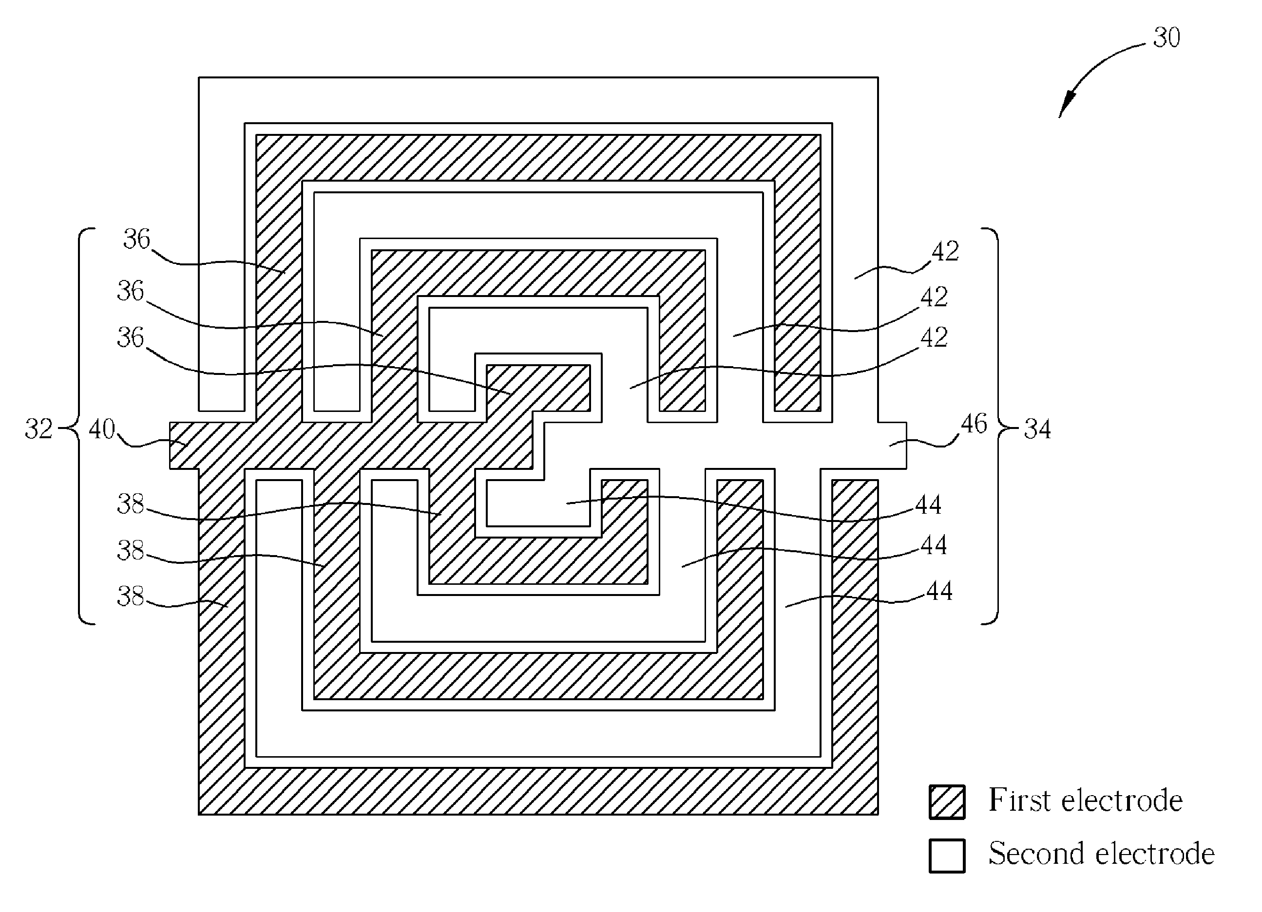
[0025]The semiconductor capacitor structures described in the embodiments of the present invention adopt the capacitor manufacturing technologies embodying metal-oxide-metal (MOM) capacitor structures, which do not require additional process cost above the standard CMOS manufacturing process, as a preferred realization scheme thereof. In other words, the capacitors in the embodiments of the present invention include metal layers as conductive material and oxide layers as dielectric material. As will be appreciated by those of ordinary skill in the pertinent art, however, the realization of the core concept of the present invention is not necessarily limited to the disclosed embodiments as hereinafter described. Other known or novel conductive materials or dielectric materials can also be applied to implement the capacitor structure of the present invention.

[0026]Please refer to FIG. 3 and FIG. 4 together. FIG. 3 is a simplified diagram of an odd metal layer 30 of a semiconductor cap...


PUM


Abstract

The present invention provides a metal-oxide-metal (MOM) capacitor structure having a plurality of symmetrical ring type sections. The MOM capacitor structure of the present invention does not need photomasks above standard CMOS process, and thus the process cost is cheaper. In addition, due to the semiconductor process improvement, a significantly large number of metal layers can be stacked in the MOM capacitor structure, and since the distance between the metal layers becomes smaller, the unit capacitance will be increased.

Description

BACKGROUND OF THE INVENTION[0001]1. Field of the Invention[0002]The present invention relates to a semiconductor capacitor structure, and more particularly, to a metal-oxide-metal (MOM) type capacitor structure having a plurality of symmetrical ring type sections.[0003]2. Description of the Prior Art[0004]In semiconductor manufacturing processes, metal capacitors constituted by metal-insulator-metal (MIM) capacitor structures are widely applied in Ultra Large Scale Integration (ULSI) designs. Due to their lower resistance, less significant parasitic effect, and absence of induced voltage shift in the depletion region, metal capacitors with MIM capacitor structure are usually adopted as the main choice of semiconductor capacitor designs.[0005]However, since the manufacturing cost for the MIM capacitor structure is very expensive, mainly due to the additional photomask(s) required in the manufacturing process, and as the cost becomes more significant along with development of advanced...

Claims


Application Information

Patent Timeline
Patent Type & Authority Applications(United States)
IPC IPC(8): H01L29/92H01L23/48
CPCH01G2/065H01G4/01H01L27/0207H01L27/0805
Inventor KANG, HAN-CHANGYEH, TA-HSUN
Owner REALTEK SEMICON CORP
Why Eureka
Try Eureka