Semiconductor Device and Method for Manufacturing Semiconductor Device

a semiconductor device and semiconductor technology, applied in the field of semiconductor devices, can solve problems such as damage to the semiconductor element of the semiconductor device, and achieve the effect of high-reliability semiconductor devices

Inactive Publication Date: 2008-10-02
SEMICON ENERGY LAB CO LTD
View PDF2 Cites 15 Cited by
  • Summary
  • Abstract
  • Description
  • Claims
  • Application Information

AI Technical Summary

Benefits of technology

[0010]By providing the plurality of projecting members over the element layers, external force applied to a semiconductor device can be reduced if applied to the semiconductor device.
[0013]By implementing the present invention, a semiconductor device having resistance to physical force from external can be provided and also a highly reliable semiconductor device can be provided.

Problems solved by technology

However, there has been a problem in that when a semiconductor device is used, impulse or stress is received by the semiconductor device and therefore a semiconductor element in the semiconductor device will be damaged.

Method used


Image

  • Semiconductor Device and Method for Manufacturing Semiconductor Device
  • Semiconductor Device and Method for Manufacturing Semiconductor Device
  • Semiconductor Device and Method for Manufacturing Semiconductor Device

Examples


embodiment mode 1

[0026]In this embodiment mode, a structural example of a semiconductor device of the present invention is described with reference to drawings.

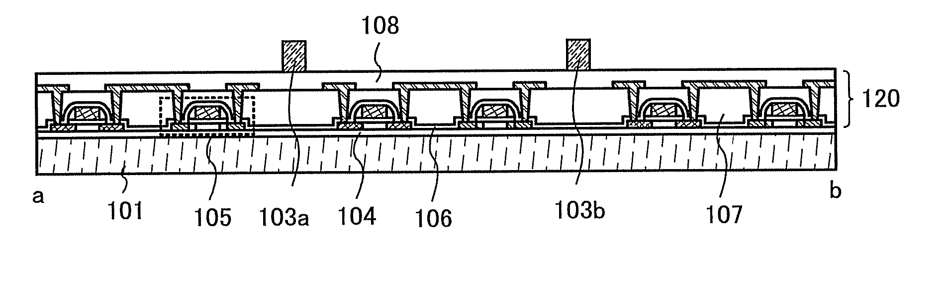
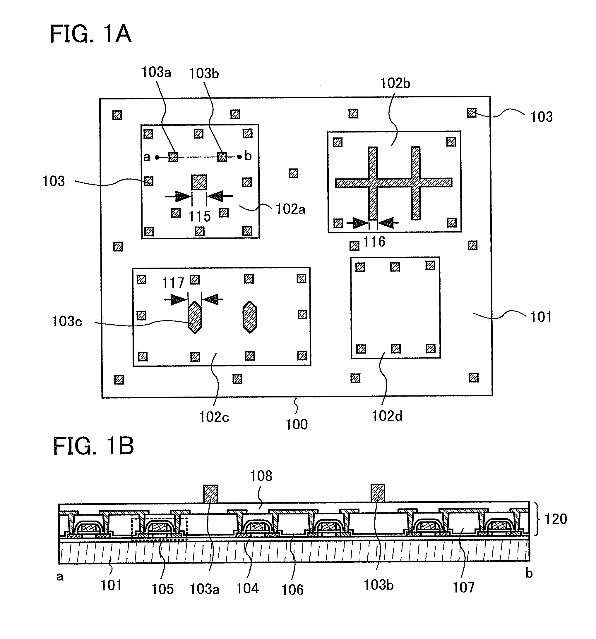
[0027]FIG. 1A shows a top structure of a semiconductor device 100 of this embodiment mode. The semiconductor device 100 includes blocks 102a to 102d provided over a substrate 101. A projecting member 103 is provided between blocks and projecting members are also provided in each of the blocks. In the case of taking a block 102a as an example, the projecting member 103 is provided in the periphery of the block 102a and projecting members are also provided in the block 102a.

[0028]The blocks 102a to 102d each include an element such as a transistor or a diode. As the diode, a variety of diodes such as a variable capacitance diode, a Schottky diode, and a tunnel diode can be applied.

[0029]Intervals at which a plurality of projecting members 103 are provided may each be set in a range of from 2 to 200 μm (preferably, from 50 to 150 μm). The plura...

embodiment mode 2

[0048]FIGS. 11A and 11B are views showing an example of a semiconductor device of this embodiment mode. This embodiment mode is similar to Embodiment Mode 1 except that openings are formed in an element layer, a plurality of projecting members are provided in the openings, and the longitudinal elastic modulus of the material of the plurality of projecting members is higher than that of the materials of a first insulating layer and a second insulating layer. A specific example of the element layer is similar to the element layer described in Embodiment Mode 1. Hereinafter, like reference numerals refer to like parts between the structure of this embodiment mode and the structure of Embodiment Mode 1, and description thereof is omitted.

[0049]First, all of the insulating films 104 to 108 of the element layer 120 are removed to form openings. Note that it is preferable that the insulating film 104 be not removed and the insulating films 106 to 108 be removed to form openings.

[0050]Proje...

embodiment mode 3

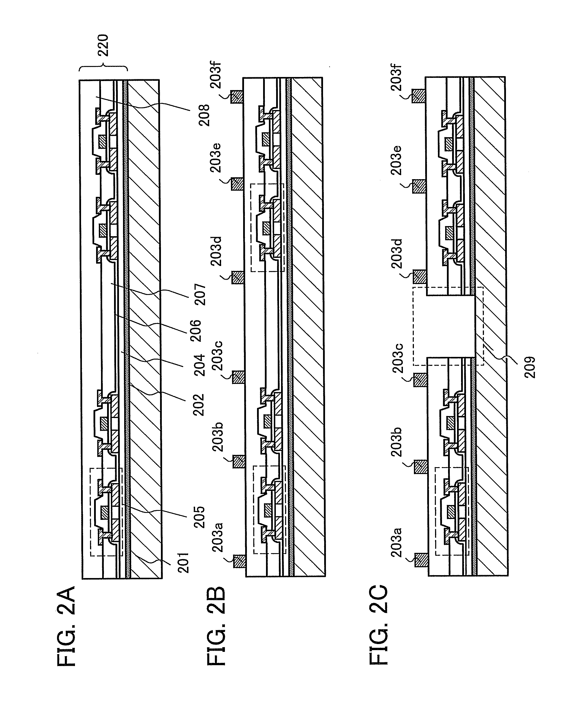
[0059]In this embodiment mode, an example of a method for manufacturing a semiconductor device of the present invention is described with reference to FIGS. 2A to 3F.

[0060]Here, an example where an element layer is provided over a substrate with a release layer interposed therebetween and then the element layer is separated from the substrate is described.

[0061]In this embodiment mode, an example where after an element layer including an element such as a transistor is provided over a rigid substrate such as a glass substrate, the element layer is separated from the rigid substrate by a release method and the element layer is provided over another substrate so that a semiconductor device is manufactured is described.

[0062]First, a release layer 202 is formed over a substrate 201 (also referred to as a first substrate), and an element layer 220 including an insulating film 204 (also referred to as a first insulating film), a thin film transistor 205 (also referred to as a TFT), an in...


PUM


Abstract

An object is to provide a semiconductor device which is not easily broken even if stressed externally and a method for manufacturing such a semiconductor device. A semiconductor device includes an element layer including a transistor in which a channel is formed in a semiconductor layer and insulating layers which are formed as an upper layer and a lower layer of the transistor respectively, and a plurality of projecting members provided at intervals of from 2 to 200 μm on a surface of the element layer. The longitudinal elastic modulus of the material for forming the plurality of projecting members is lower than that of the materials of the insulating layers. (111 words)

Description

BACKGROUND OF THE INVENTION[0001]1. Field of the Invention[0002]The present invention relates to semiconductor devices and a method for manufacturing the semiconductor devices.[0003]2. Description of the Related Art[0004]In recent years, a semiconductor device, or the like using a semiconductor element formed over a rigid substrate such as a glass substrate has been actively developed for use in a display such as an LCD or an organic EL display, a photoelectric conversion element such as a photo sensor or a solar cell, or the like. Further, a semiconductor device which transmits and receives data without contact (also referred to as an RFID (radio frequency identification) tag, an ID tag, an IC tag, an IC chip, a wireless tag, an electronic tag, or a wireless chip) has been actively developed. Further, these days, flexible devices such as a film display and a semiconductor device embedded in paper have been required (Patent Document 1: Japanese Published Patent Application No. 2005-...

Claims


Application Information

Patent Timeline
Patent Type & Authority Applications(United States)
IPC IPC(8): H01L23/58H01L21/30
CPCH01L23/3121H01L23/3135H01L23/562H01L23/66H01L2223/6677H01L2924/19041H01L2924/0002H01L2924/00
Inventor OHNUMA, HIDETO
Owner SEMICON ENERGY LAB CO LTD
Why Eureka
Try Eureka