
Electronic meter having user-interface and central processing functionality on a single printed circuit board

a technology of electronic meter and printed circuit board, which is applied in the direction of printed circuit board receptacles, liquid/fluent solid measurement, instruments, etc., can solve the problems of increasing the size of ied by additional processors and specialized hardware, and affecting the quality of ied, etc., and achieves the effect of small footprint and easy assembly

Active Publication Date: 2008-10-02
ELECTRO INDUSTRIES GAUGE TECH
View PDF9 Cites 79 Cited by
  • Summary
  • Abstract
  • Description
  • Claims
  • Application Information

AI Technical Summary

Benefits of technology

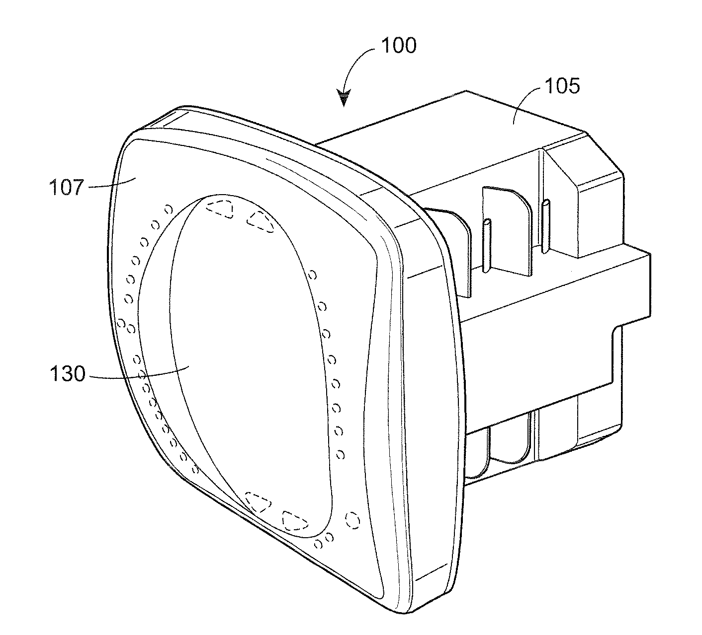
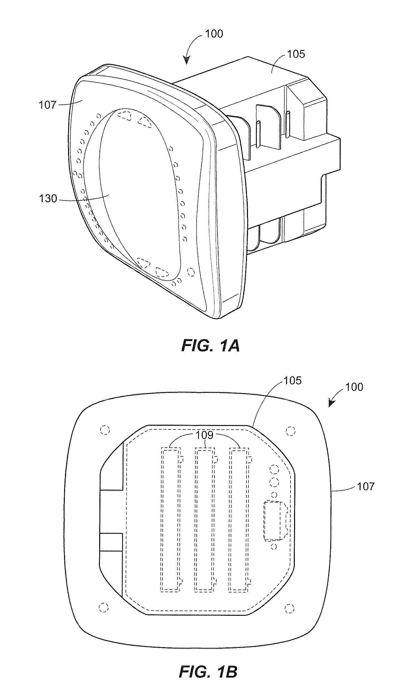
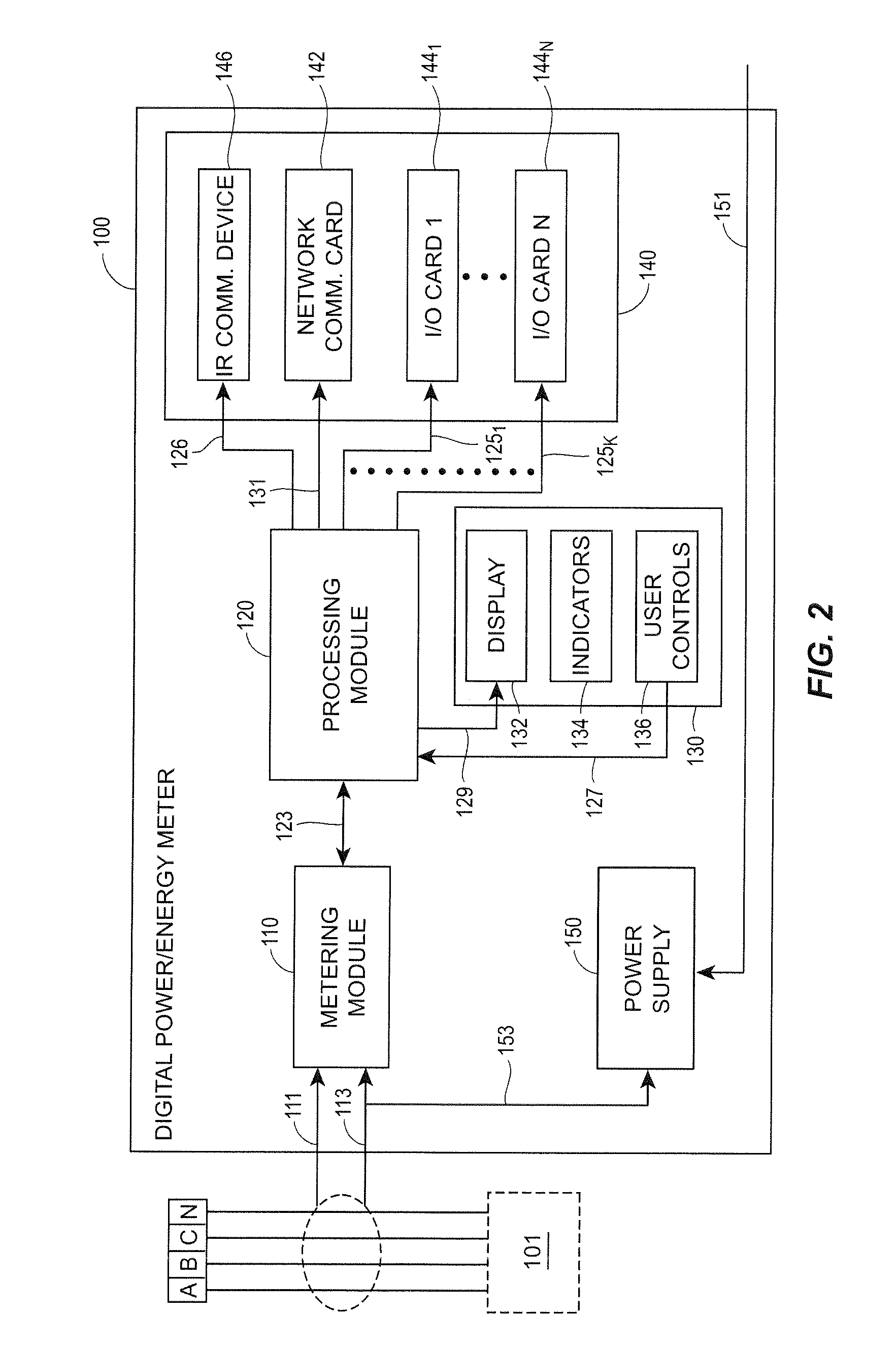
The patent describes a smaller and easier to assemble digital electrical power and energy meter. The meter includes a motherboard and a plurality of interface boards. The motherboard has a user interface and the main processing hardware for the meter, and the interface boards connect to the motherboard. The patent provides techniques for mounting components on a single printed circuit board motherboard, which avoids the use of three printed circuit boards. The user can utilize advanced technology such as Ethernet and expandable I / O that fits easily into existing enclosures where analog meters were used. The technical effects of the patent are a smaller, easier to assemble, and advanced meter that can be retro fitted into existing enclosures.

Problems solved by technology

However, this is not always true.
Additional processors and specialized hardware necessarily increase the size of the IED.
These types of improvements have been hampered because of physical space limitations on a printed circuit board.
While through-hole mounting provides strong mechanical bonds, the additional drilling required makes the board more expensive to produce.
It also limits the available routing area for signal traces on layers immediately below the top layer on multilayer boards since the holes must pass through all layers to the opposite side.
Furthermore, components mounted by this technique makes it virtual impossible to mount additional components on the opposite side of the board.
Due to the fact that all these connectors were used to connect the boards together, the space on these printed circuit boards was used inefficiently.
This made the power meters bulky and large and difficult to retrofit within existing analog enclosures.

Method used


Image

  • Electronic meter having user-interface and central processing functionality on a single printed circuit board
  • Electronic meter having user-interface and central processing functionality on a single printed circuit board
  • Electronic meter having user-interface and central processing functionality on a single printed circuit board

Examples


Embodiment Construction

[0018]Although the following text sets forth a detailed description of numerous embodiments, it should be understood that the legal scope of the present disclosure is defined by the words of the claims set forth at the end of this patent. The detailed description is to be construed as exemplary only and does not describe every possible embodiment, as describing every possible embodiment would be impractical, if not impossible. One could implement numerous alternate embodiments, using either current technology or technology developed after the filing date of this patent, which would still fall within the scope of the claims.

[0019]It should also be understood that, unless a term is expressly defined in this patent using the sentence “As used herein, the term ‘______’ is hereby defined to mean . . . ” or a similar sentence, there is no intent to limit the meaning of that term, either expressly or by implication, beyond its plain or ordinary meaning, and such term should not be interpre...


PUM


Abstract

A digital electrical power and energy meter integrates a primary processing module and a user interface module onto a single printed circuit board to reduce overall meter size, assembly time, and cost.

Description

CROSS-REFERENCE TO RELATED PATENTS AND PATENT APPLICATIONS[0001]This application claims priority to U.S. Provisional Patent Application No. 60 / 920,128, filed on Mar. 27, 2007, which is herein incorporated by reference.FIELD[0002]The present disclosure relates generally to the field of intelligent electronic devices for electrical utility services and, more specifically, to digital electrical power and energy meters for electrical utility services.BACKGROUND[0003]Producers, suppliers, and consumers of electrical power rely on energy meters to monitor power consumption and quality for numerous purposes, including billing, revenue, power distribution management, and process management. Traditionally, the primary means of measuring power consumption was an electromechanical power meter. A number of other types of meters and equipment measured other parameters of power generation, distribution, usage, and quality. As technology has improved, intelligent electronic devices (IEDs), such as...

Claims


Application Information

Patent Timeline
Patent Type & Authority Applications(United States)
IPC IPC(8): G08B23/00
CPCG01R22/06G01R22/065H05K7/1424G01D18/008G01R21/00G01R35/00
Inventor BANHEGYESI, TIBORKAGAN, ERRAN
Owner ELECTRO INDUSTRIES GAUGE TECH
Learn More