Display apparatus, display-apparatus driving method and electronic equipment

a technology for display apparatus and electronic equipment, applied in static indicating devices, instruments, electroluminescent light sources, etc., can solve the problems of difficulty in allocating sufficient time to each threshold-voltage correction operation, loss of uniformity of screen, etc., to suppress the variation of driving transistor characteristics, high reliability, and high degree of reliability

Active Publication Date: 2008-10-02
JOLED INC
View PDF1 Cites 20 Cited by
  • Summary
  • Abstract
  • Description
  • Claims
  • Application Information

AI Technical Summary

Benefits of technology

[0018]In order to solve the problems described above, inventors of the present invention have innovated a display apparatus capable of allocating sufficient time to each of the threshold-voltage correction operation and the mobility correction operation as a threshold-voltage correction period and a mobility correction period respectively so as to assure that the threshold-voltage correction operation and the mobility correction operation can be carried out with a high degree of reliability. In addition, the inventors have also innovated a driving method for the display apparatus and electronic equipment employing the display apparatus.
[0020]In the display apparatus having the configuration described above as well as electronic equipment employing the display apparatus, as explained above, before a threshold-voltage correction operation is carried out on the pixel row in a horizontal scan period, a preparatory operation is carried out on the pixel row prior to the horizontal scan period in order to fix each of an electric potential appearing on the gate of the driving transistor and an electric potential appearing on the source of the driving transistor at a predetermined level. Thus, it is no longer necessary to allocate sufficient time of the horizontal scan period provided for the pixel row subjected to the threshold-voltage correction operation to the threshold-voltage correction preparatory operation as a threshold-voltage correction preparation period. Therefore, the threshold-voltage correction period set in the horizontal scan period can be prolonged by the threshold-voltage correction preparation period. As a result, it is possible to allocate sufficient time to the threshold-voltage correction operation as a threshold-voltage correction period so as to assure that the threshold-voltage correction operation can be carried out with a high degree of reliability.
[0021]In accordance with the embodiment of the present invention, it is possible to allocate sufficient time to the threshold-voltage correction operation as a threshold-voltage correction period so as to assure that the threshold-voltage correction operation in order to suppress variations of the characteristics of the driving transistor and deteriorations of the electro-optical device with the lapse of time can be carried out with a high degree of reliability. Thus, an image having a high quality can be displayed.

Problems solved by technology

Thus, in the present state of the art, it is difficult to allocate sufficient time to each of the threshold-voltage correction operation and the mobility correction operation as a threshold-voltage correction period and a mobility correction period respectively.
It is to be noted, however, that an organic EL display apparatus with a configuration including pixel circuits each having only the threshold-voltage correction function also raises the problem of difficulty to allocate sufficient time to the threshold-voltage correction operation as a threshold-voltage correction period as is the case with the organic EL display apparatus with a configuration including pixel circuits each having both the threshold-voltage correction function and the mobility correction function.
Thus, even if a uniform voltage is applied to the gates of driving transistors, uniformity of the screen is lost due to variations of the luminance of a light beam generated by the organic EL device from pixel to pixel.

Method used


Image

  • Display apparatus, display-apparatus driving method and electronic equipment
  • Display apparatus, display-apparatus driving method and electronic equipment
  • Display apparatus, display-apparatus driving method and electronic equipment

Examples


Embodiment Construction

[0044]Preferred embodiments of the present invention are described in detail by referring to diagrams as follows.

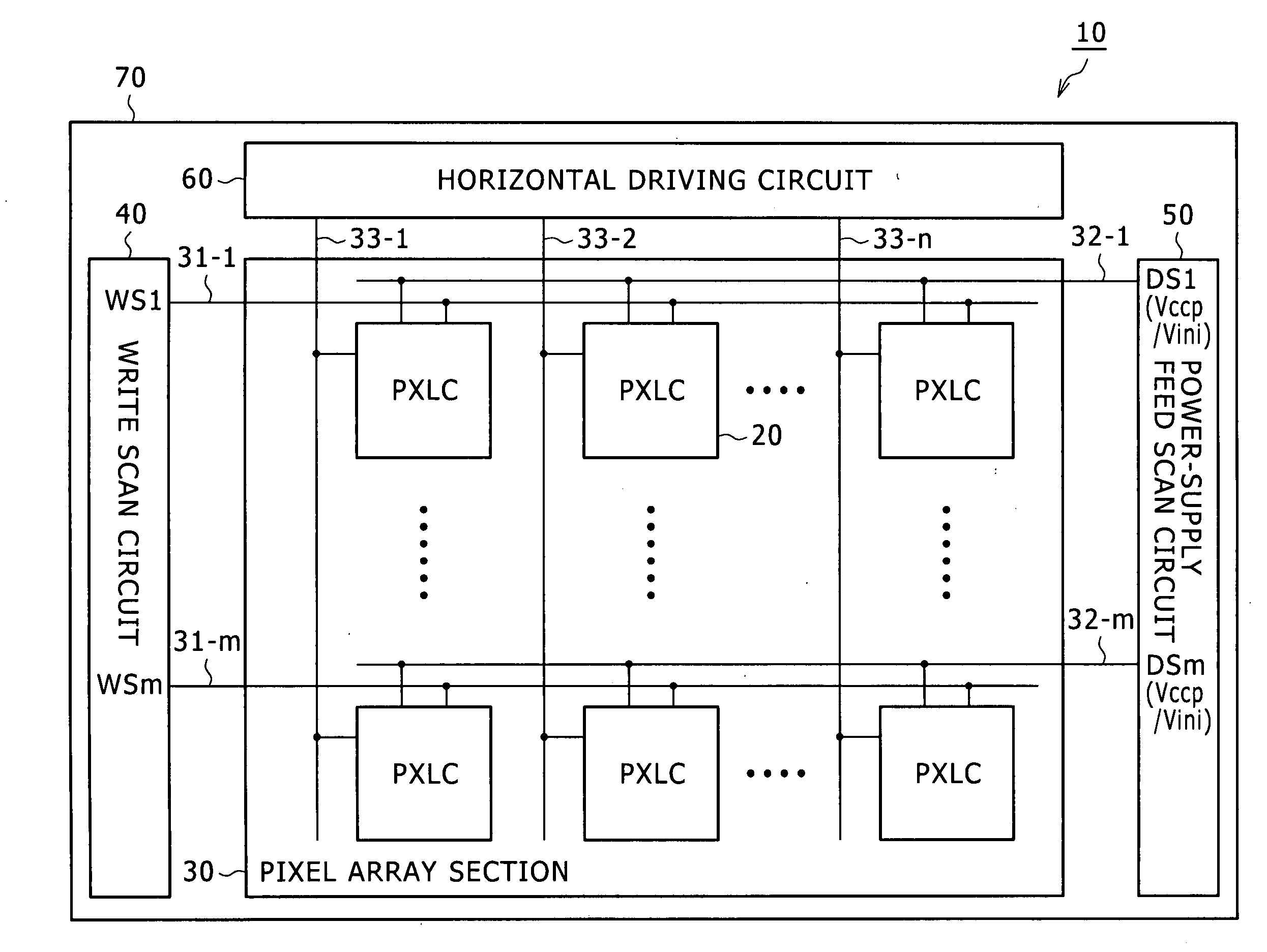
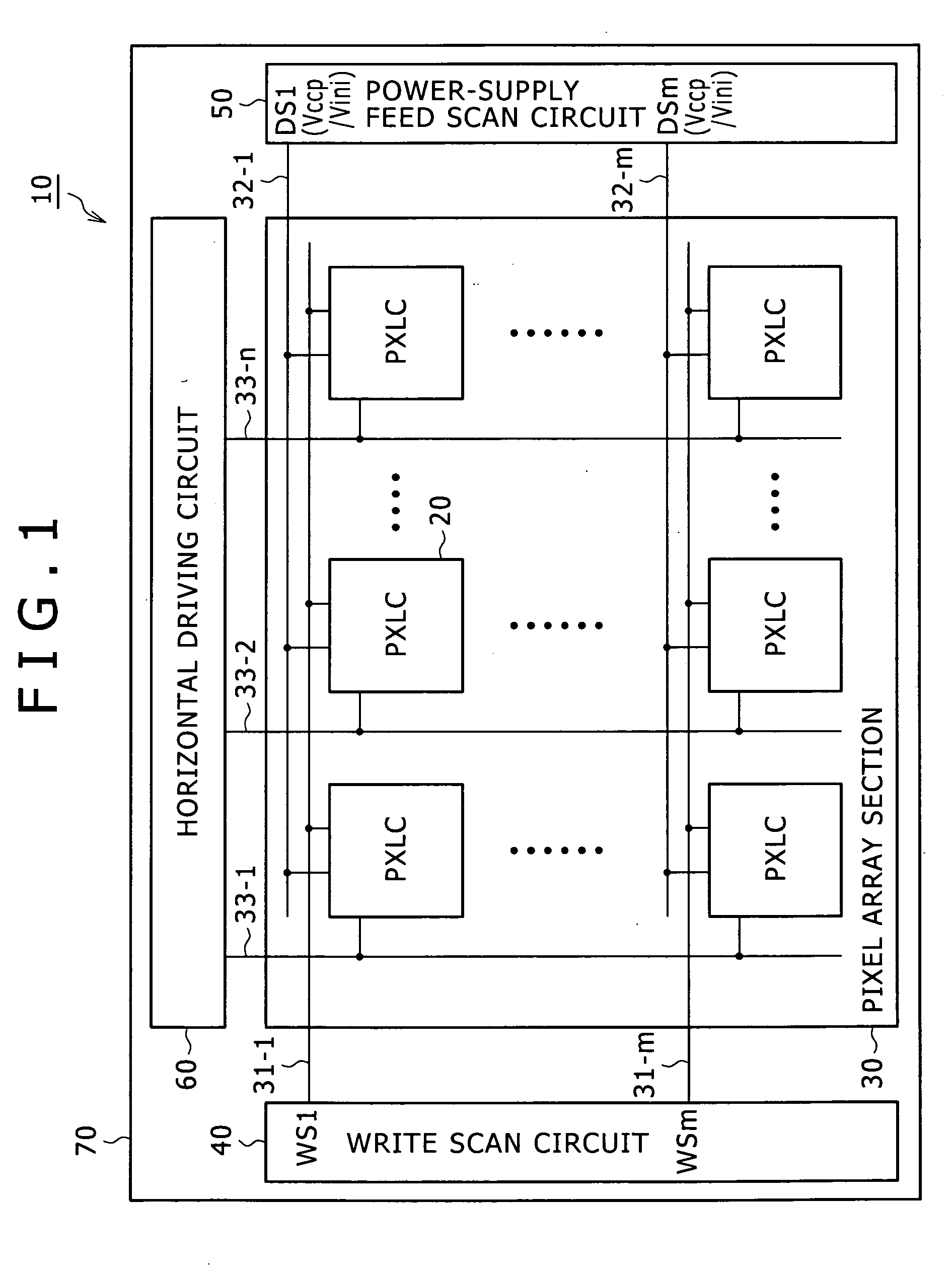
[0045]FIG. 1 is a system configuration diagram roughly showing the configuration of an active-matrix display apparatus according to an embodiment of the present invention. This typical configuration includes current-driven electro-optical devices each generating a light beam with the luminance thereof determined by a current flowing through the device. That is to say, the typical active-matrix display apparatus is an active-matrix organic EL display apparatus 10 employing light emitting devices each serving as the electro-optical device. An example of the light emitting device employed as the electro-optical device is an organic EL device.

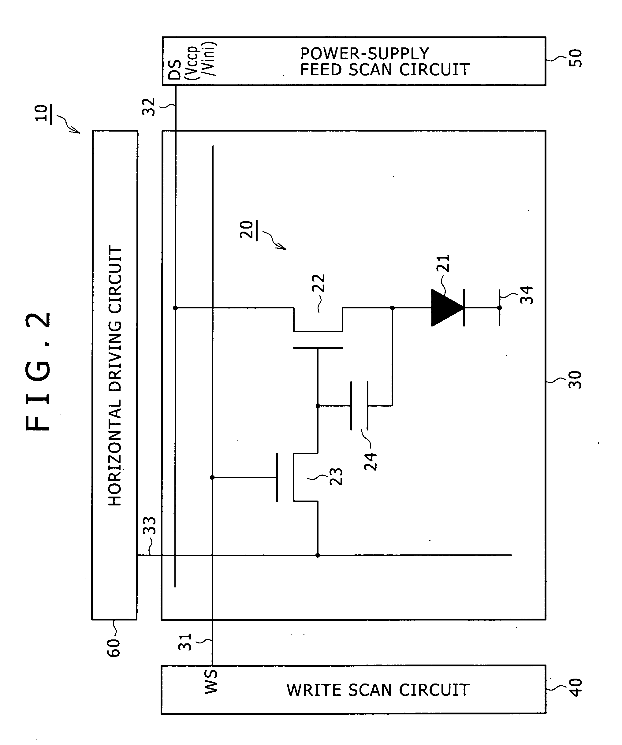
[0046]As shown in FIG. 1, the organic EL display apparatus 10 according to the embodiment employs a pixel array section 30 including pixel circuits (PXLC) 20 laid out two-dimensionally to form a matrix and a driving section placed in the...


PUM


Abstract

In the present invention, there is provided a display apparatus including: a pixel array section including pixel circuits each having an electro-optical device, a write transistor configured to carry out a voltage storing process to sample a video signal and store the sampled video signal, a holding capacitor configured to hold the sampled video signal, and a driving transistor configured to drive the electro-optical device; and a driving circuit configured to carry out a selective scan operation on the pixel circuits in row units, and a threshold-voltage correction operation to correct variations of the threshold voltage of every driving transistor wherein, before the driving circuit carries out a threshold-voltage correction operation in a horizontal scan period, the driving circuit performs a preparatory operation prior to the horizontal scan period in order to fix each of electric potentials appearing on the gate and the source of the driving transistor at a predetermined level.

Description

CROSS REFERENCES TO RELATED APPLICATIONS[0001]The present invention contains subject matter related to Japanese Patent Application JP 2007-079037 filed in the Japan Patent Office on Mar. 26, 2007, the entire contents of which being incorporated herein by reference.BACKGROUND OF THE INVENTION[0002]1. Field of the Invention[0003]The present invention relates to a display apparatus, a method for driving the display apparatus and electronic equipment. More particularly, the present invention relates to a display apparatus of a flat-panel type, in which pixel circuits each including an electro-optical device are laid out to form a matrix, a method for driving the display apparatus and electronic equipment employing the display apparatus.[0004]2. Description of the Related Art[0005]In recent years, in the field of a display apparatus for displaying an image, a display apparatus of a flat-panel type, in which pixels (or pixel circuits) each including a light emitting device are laid out to...

Claims


Application Information

Patent Timeline
Patent Type & Authority Applications(United States)
IPC IPC(8): G06F3/038G09G3/34
CPCG09G3/3233G09G2300/043G09G2300/0819G09G2300/0866G09G2310/0262G09G2310/0297G09G2320/043G09G2320/045G09G3/30G09G3/20G09G3/32H05B33/12
Inventor TANEDA, TAKAYUKIYAMAMOTO, TETSUROIIDA, YUKIHITOUCHINO, KATSUHIDE
Owner JOLED INC
Why Eureka
Try Eureka