Method for fabricating semiconductor device

a semiconductor and device technology, applied in the direction of coatings, metallic material coating processes, chemical vapor deposition coatings, etc., can solve the problems of unsatisfactory layer, serious deformation of transistor performance, and greatly increased native oxide, so as to reduce eot and increase device performance

Inactive Publication Date: 2008-10-02
TAIWAN SEMICON MFG CO LTD
View PDF9 Cites 4 Cited by
  • Summary
  • Abstract
  • Description
  • Claims
  • Application Information

AI Technical Summary

Benefits of technology

[0008]The invention provides a method for fabricating a semiconductor device capable of reducing EOT and increasing device performance by preventing the formation of metal oxide resulting from exposure to the ambient.

Problems solved by technology

In the ambient environment, the substrates are exposed to mechanical and chemical contaminants, such as particles, moisture and others, that may damage the gate electrode being fabricated and possibly form an undesired layer, such as, a native oxide layer.
In 65 nm technology node, inventor observed that native oxide is greatly increased and performance of transistor is seriously degraded.

Method used


Image

  • Method for fabricating semiconductor device
  • Method for fabricating semiconductor device
  • Method for fabricating semiconductor device

Examples


Embodiment Construction

[0017]The following description is of the best-contemplated mode of carrying out the invention. This description is made for the purpose of illustrating the general principles of the invention and should not be taken in a limiting sense. The scope of the invention is best determined by reference to the appended claims.

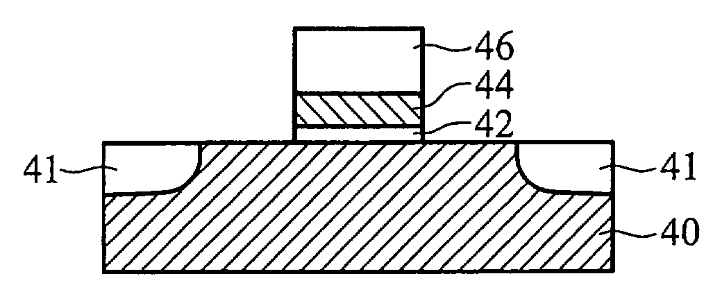
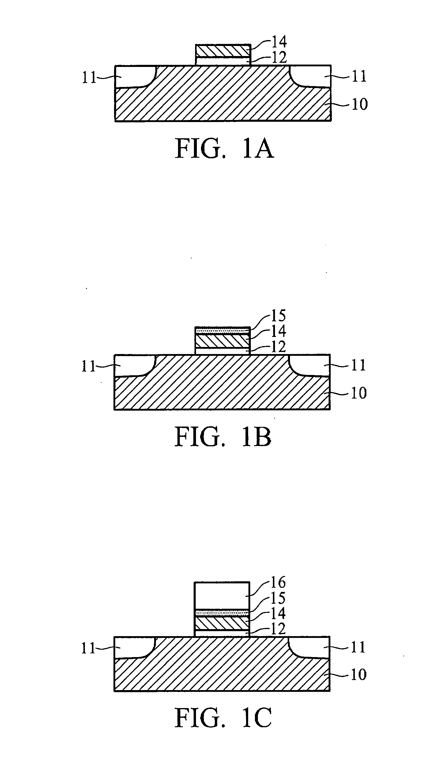
[0018]The invention provides a method for fabricating a semiconductor device by in-situ deposition of a metallic film and a silicon-containing film to avoid formation of metal oxide. In one embodiment, the metallic film and the silicon-containing film are deposited in different chambers of a single cluster tool system. In another embodiment, the metallic film and the silicon-containing film are deposited in different chambers of two cluster tool systems. The metallic film can be deposited by a chemical vapor deposition (CVD), physical vapor deposition (PVD), low pressure chemical vapor deposition (LPCVD), plasma enhanced chemical vapor deposition (PECVD) or atomic laye...


PUM

PropertyMeasurementUnit
thicknessaaaaaaaaaa
dielectric constantaaaaaaaaaa
pressureaaaaaaaaaa

Abstract

A method for fabricating a semiconductor device is disclosed. The method includes providing a first chamber and a second chamber. The first chamber and the second chamber are connected by a pressure differential unit, for depositing a metallic film over a substrate in the first chamber, transferring the substrate to the second chamber via the pressure differential unit without exposing the substrate to the ambient environment, and depositing a silicon-containing film on the metallic film in the second chamber.

Description

BACKGROUND OF THE INVENTION[0001]1. Field of the Invention[0002]The invention relates to a method for fabricating a semiconductor device, and more particularly to a method for fabricating a metal electrode capable of eliminating surface oxidation due to the ambient environment.[0003]2. Description of the Related Art[0004]A metal oxide semiconductor field effect transistor (MOSFET) comprises a gate structure disposed between source and drain regions formed in a substrate. The gate structure typically comprises a gate electrode and a gate dielectric. The gate electrode is disposed over the gate dielectric to control a flow of charge carriers in a channel region formed between the drain and source regions under the gate dielectric. To reduce equivalent oxide thickness (EOT) at the 65 nm generation technology node and beyond, the gate dielectric may be formed from a material having a dielectric constant greater than 4. Materials for forming the gate electrode may comprise metal. Such di...

Claims


Application Information

Patent Timeline
Patent Type & Authority Applications(United States)
IPC IPC(8): H01L21/46
CPCH01L21/28079H01L21/28088H01L21/67207
Inventor CHANG, WENGYEN, FONG-YUTAO, HUN-JANLIANG, MONG-SONG
Owner TAIWAN SEMICON MFG CO LTD
Why Eureka
Try Eureka