Electromagnetic Wave Shielding Device

a shielding device and electromagnetic wave technology, applied in the direction of magnetic/electric field screening, layered products, electric devices, etc., can solve the problems of increasing the electromagnetic interference (emi), unable to remove electromagnetic waves generated from the screen of the image displaying device, and inadequacies in covering with metal plates, etc., to achieve excellent electromagnetic wave shielding properties, prevent lifting or peeling, and proper transparency

Inactive Publication Date: 2008-10-09
DAI NIPPON PRINTING CO LTD
View PDF7 Cites 17 Cited by
  • Summary
  • Abstract
  • Description
  • Claims
  • Application Information

AI Technical Summary

Benefits of technology

[0019]According to the present invention, an electromagnetic wave shielding device can be provided, which can exhibit an excellent electromagnetic wave shielding property, a proper transparency (transmittance of visible light), as well as, ability of preventing lifting or peeling between the electromagnetic wave shielding layer and the transparent resin layer during the production processes as well as over the period of actual time of use.
[0020]According to the present invention, an electromagnetic wave shielding material can be provided, in which the material to be used for the transparent resin layer can be reduced to a small amount, in which a share in forming the transparent resin layer can be accepted to some extent, in which lifting or peeling between the layers constituting the electromagnetic wave shielding material can be prevented during the production processes as well as over the period of actual time of use, and in which a lack of the transparent resin layer on the mesh portion facing a screen portion does not occur even in the presence of some variation in the coated position of the transparent resin layer.
[0021]According to the present invention, an electromagnetic wave shielding material can be provided, in which the transparent substrate and the electromagnetic wave shielding layer laminated via the adhesive layer can be firmly adhered to each other, and the adhesive layer exposed at the bottom faces of the mesh portion and the openings can also firmly adhere the transparent resin layer filling the openings to the laminated layers, so that the effect of preventing lifting or peeling between these layers constituting the electromagnetic wave shielding material during the production processes as well as over the period of actual time of use can be secured.

Problems solved by technology

(Background Art) In recent years, with functional advance and increased utilization of electrical and electric equipments, the problems due to the electro magnetic interference (EMI) have been increased.
While these methods are effective for shielding electromagnetic waves in relation to circuits or power source blocks, they cannot remove electromagnetic waves generated from a screen of an image displaying device, such as CRTs or PDPs, and the covering with a metal plate is not appropriate because it is not transparent.
However, in the electromagnetic wave shielding sheet constructed by providing a transparent resin layer on a metal mesh, there has been found a problem that lifting or peeling may occur between the metal mesh and the transparent resin layer through all the processes from the production of the sheet to the assembly into an image displaying device as well as over a long period of the actual time of use.
Therefore, possibility that peeling will occur at this portion becomes high.
However, in fact, after having actually tried to produce the electromagnetic wave shield material based on these prior arts, we found that a new challenge to be further solved still remains.

Method used


Image

  • Electromagnetic Wave Shielding Device
  • Electromagnetic Wave Shielding Device
  • Electromagnetic Wave Shielding Device

Examples


example 1

[0089]As the electromagnetic wave shielding layer 15, an electrically conductive material formed by successively laminating a blackened layer of copper-cobalt particles with an average particle size of 0.3 μm and then a chromate-treated layer on an electrolytically produced copper foil with a thickness of 10 μm was used. After laminating the chromate-treated layer of copper-cobalt particles on the transparent substrate 11 composed of a biaxially oriented PET film A4300 (trade name of polyethylene terephthalate produced by TOYOBOSEKI Co., Ltd.) with a thickness of 100 μm using the two-part curable urethane-type adhesive 13, aging was performed for four days at 56° C. As the adhesive agent, a two-part curable urethane-type adhesive composed of a polyester urethane polyol as a basic material and a xylylene-diisocyanate as a curing agent was used in a coating amount such that the thickness after dried became 7 μm.

[0090]A line for producing shadow masks for color TVs which performs treat...

example 2

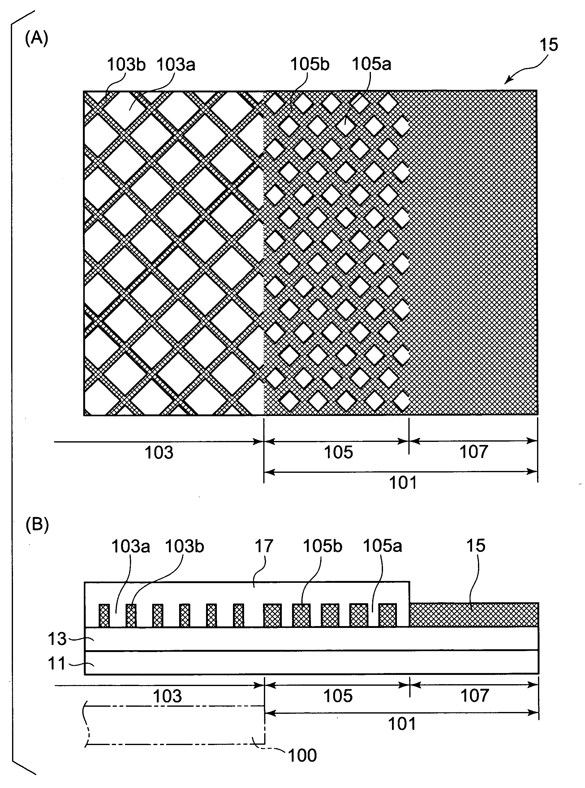
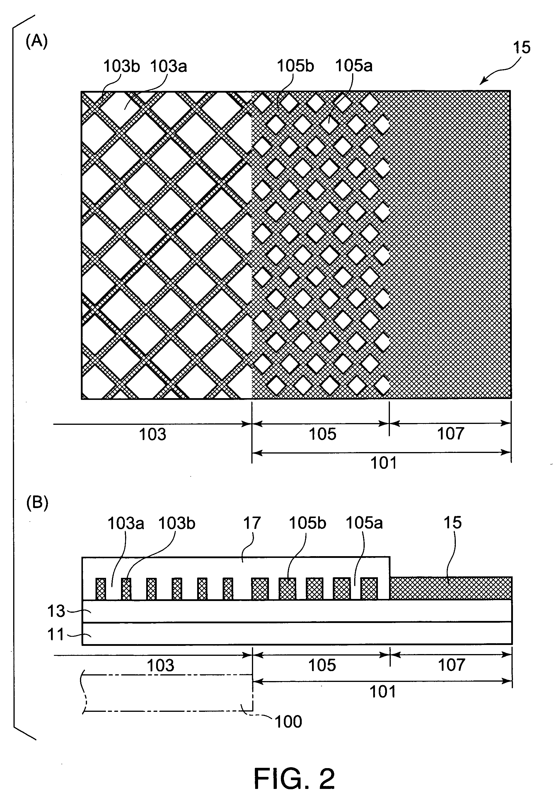
[0096]The composition of the transparent resin layer 17 was applied on the mesh portion 103 as well as on a 2.5 mm wide portion of the transparent resin layer anchoring portion 105 around the periphery of the mesh portion 103. Except these conditions, similar to the Example 1, an electromagnetic wave material according to Example 2 could be obtained, in which the transparent resin layer 17 was applied to cover and smooth over the openings 103a of the mesh portion 103 and a portion of the openings 105a of the transparent resin layer anchoring portion 105, as shown in FIG. 3(B). In this case, in the outer periphery of the transparent resin layer anchoring portion 105, the opening 105a remained still being exposed over a 2.5 mm width.

example 3

[0097]The composition of the transparent resin layer 17 was applied on the mesh portion 103 as well as on a total 5.5 mm wide portion including the transparent resin layer anchoring portion 105 and an outer surrounding portion. Except these conditions, similar to the Example 1, an electromagnetic wave material according to Example 3 could be obtained, in which the transparent resin layer 17 was applied to cover over the openings 103a of the mesh portion 103, the openings 105a of the transparent resin layer anchoring portion 105 as well as a 0.5 mm wide inner periphery (corresponding to 1.7 cycles of the openings) of the frame portion 107.


PUM


Abstract

An electromagnetic wave shielding layer 1 comprises a transparent substrate 11, an adhesive layer 13 which is provided as needed, an electromagnetic wave shielding layer 15, and a transparent resin layer 17. The electromagnetic shielding layer 15 includes a mesh portion 103 facing a screen portion 100 of an image displaying device, a transparent resin layer anchoring portion 105 surrounding a periphery of the mesh portion 103 and including openings 105a having an opening ratio lower than that of openings 103a of the mesh portion 103, and a frame portion 107 surrounding an outer periphery of the transparent resin layer anchoring portion 105 and not having openings. The transparent resin layer 17 is provided such that it covers the surfaces of the mesh portion 103 and the transparent resin layer anchoring portion 105 and fills the openings 103a, 105a.

Description

BACKGROUND OF THE INVENTION[0001]The present invention relates to a sheet adapted to shield electromagnetic waves, and particularly to an electromagnetic wave shielding material (electromagnetic shielding device) disposed on a front surface of an image displaying device (display), such as CRTs or PDPs, and adapted to shield electromagnetic waves generated from the image displaying device.FIELD OF THE INVENTION[0002]As used herein, the term, “image displaying device”, means “display”, “CRT” means “Cathode Ray Tube (Braun tube)”, and “PDP” means “Plasma Display Panel”, and these terms are used as abbreviations, functional expressions, commonly known names or industrial terminologies.BACKGROUND ART[0003](Background Art) In recent years, with functional advance and increased utilization of electrical and electric equipments, the problems due to the electro magnetic interference (EMI) have been increased. A variety of image displaying devices are also generating sources of EMI. For examp...

Claims


Application Information

Patent Timeline
Patent Type & Authority Applications(United States)
IPC IPC(8): H05K9/00
CPCB32B7/02H05K9/0096B32B7/025
Inventor NAITO, NOBUOARAKAWA, FUMIHIROFUJII, KAZUHITO
Owner DAI NIPPON PRINTING CO LTD
Why Eureka
Try Eureka