Process for preparing light transmissive electromagnetic wave shielding material, light transmissive electromagnetic wave shielding material and display filter

a technology of electromagnetic shielding material and light transmission, which is applied in the manufacture of electrode systems, cold cathode manufacturing, and discharge tube/lamp manufacture. it can solve the problems of electromagnetic wave occurrence, precision equipment malfunction, and affect the human body, and achieve high adhesion, uniform thickness, and high dimensional accuracy.

Inactive Publication Date: 2011-04-26
BRIDGESTONE CORP
View PDF7 Cites 9 Cited by
  • Summary
  • Abstract
  • Description
  • Claims
  • Application Information

AI Technical Summary

Benefits of technology

[0030]The metal conductive layer having a microscopic pattern and a uniform thickness can be formed with a high dimensional accuracy by using the pretreatment agent for electroless plating of the invention comprising a noble metal compound, a silane coupling agent and an azole compound to form the pretreatment layer, and forming the metal conductive layer on the pretreatment layer. In addition, the noble metal compound, the silane coupling agent and the azole compound are dispersed at the atomic level, so that the pretreatment layer having no a crack and a fog is formed. The pretreatment agent for electroless plating preferably further comprises a synthetic resin. This pretreatment agent can form the pretreatment layer having a high adhesion to the transparent substrate and the metal conductive layer. In addition, the pretreatment layer having the high adhesion enables the formation of the metal conductive layer with a high dimensional accuracy.
[0031]Therefore, the process of the present invention provides a light transmissive electromagnetic wave shielding material having an excellent light transmissive property, an excellent electromagnetic wave shielding property, an excellent appearance property and an excellent visibility.

Problems solved by technology

In recent years, along with the popularization of office automation equipments and communication equipments, there is fear that an electromagnetic wave generated by the equipments has an affect on the human body.
In addition, the electromagnetic wave generated by a cell-phone may cause a precision equipment to malfunction.
Therefore, the occurrence of the electromagnetic wave is of a problem to be solved.
However, it was difficult for the conventional light transmissive electromagnetic wave shielding material to balance the light transmissive property with the electromagnetic wave shielding property.
This is, it is difficult for the light transmissive electromagnetic wave shielding material (1) to have the microscopic mesh pattern due to limitation for minimizing the line and distortion of line arrangement.
The light transmissive electromagnetic wave shielding material (2) has problems that the electromagnetic wave shielding property is not enough and the metallic luster is too high.
The light transmissive electromagnetic wave shielding material (3) has problems that the production process is long, the cost is high, and the light transmissive property is reduced by an adhesive layer arranged between the transparent substrate and the copper layer.
In addition, the light transmissive electromagnetic wave shielding material (4) has problems that the electromagnetic wave shielding property is low.

Method used


Image

  • Process for preparing light transmissive electromagnetic wave shielding material, light transmissive electromagnetic wave shielding material and display filter
  • Process for preparing light transmissive electromagnetic wave shielding material, light transmissive electromagnetic wave shielding material and display filter

Examples


example 1-1

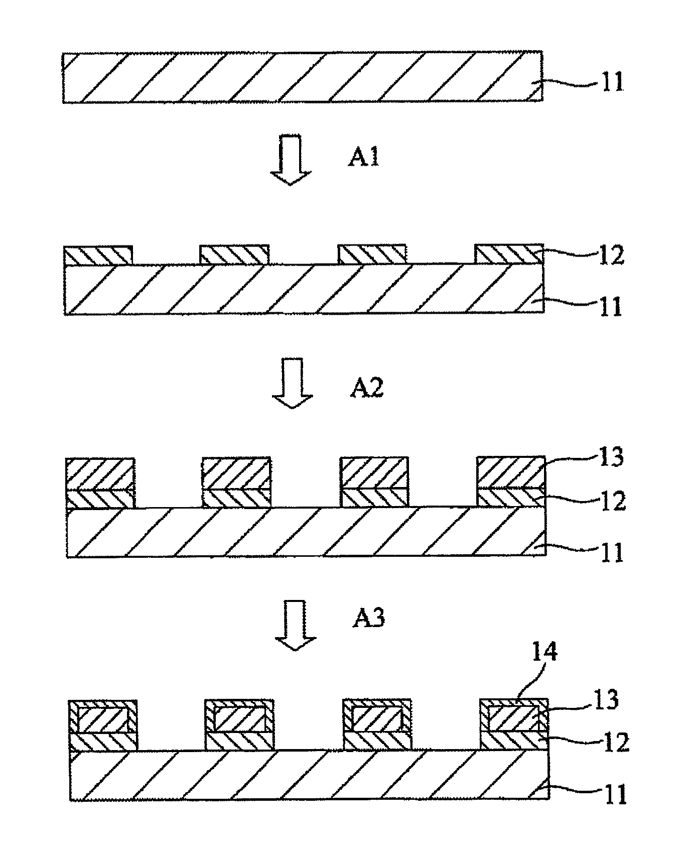
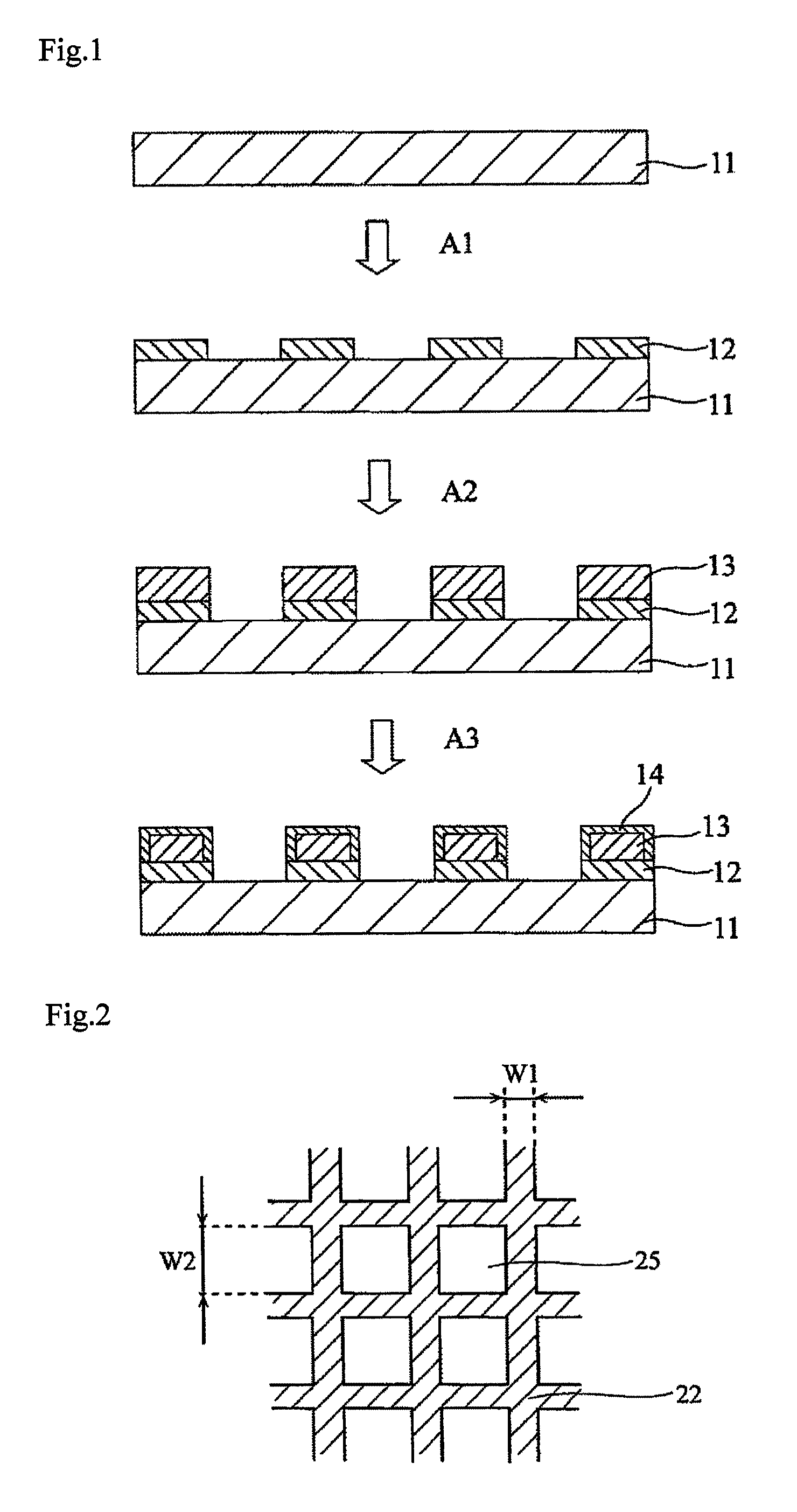
1. Preparation of a Pretreatment Agent

[0120]γ-Glycidoxypropyltrimethoxysilane was added to imidazole at a mole ratio of 1:1, and reacted for an hour and for 100 minutes, to prepare a reaction product. Palladium chloride was added to a 5 wt % aqueous solution of the reaction product with stirring at 25° C. to prepare a solution having palladium chloride concentration of 10 g / L. This solution was diluted with n-butanol by 100-fold by volume to prepare a pretreatment agent having palladium chloride concentration of 100 mg / L.

2. Formation of a Mesh-Shaped Preparation Layer

[0121]The pretreatment agent was printed in a mesh pattern on a PET film (the thickness of 100 μm) by gravure printing, and then dried at 120° C. for 5 minutes to form a mesh-shaped pretreatment layer. The pretreatment layer had a line width of 20 μm, a line pitch of 235 μm, an aperture ratio of 85% and a thickness of 0.15 μm.

3. Formation of the Metal Conductive Layer

[0122]The PET film on which the pretreatment layer ha...

example 1-2

[0131]The PET film on which the pretreatment layer had been formed by the same manner as the example 1-1 was immersed in an electroless plating copper solution (Melpate CU-5100 manufactured by Meltex Co., Ltd) and subjected to electroless plating treatment at 50° C. for 5 minutes to form a mesh-shaped metal conductive layer. Then the PET film was immersed in an aqueous solution of copper sulfate for electrolytic plating and applied electrical current (the current density of 2 A / dm2) to it by a rectifier for 5 minutes to form a mesh-shaped metal conductive layer. The metal conductive layer had a line width of 28 μm, a line pitch of 227 μm, an aperature ratio of 79% and a thickness of 4 μm.

[0132]Then the metal conductive layer was subjected to a blackening treatment by the same manner as the example 1-1 to provide a light transmissive electromagnetic wave shielding material having the metal conductive layer whose surface was subjected to the blackening treatment.

example 1-3

[0133]The PET film on which the pretreatment layer had been formed by the same manner as the example 1-1 was immersed in a nickel-boron alloy electroless plating solution (Top Chemialloy B-1 manufactured by OKU-NO CHEMICAL INDUSTRIES Co., Ltd) and subjected to electroless plating treatment to form a mesh-shaped metal conductive layer at 60° C. for 5 minutes. Then the PET film was immersed in an aqueous solution of copper sulfate for electrolytic plating and applied electrical current (the current density of 2 A / dm2) to it by a rectifier for 5 minutes to form a mesh-shaped metal conductive layer. The metal conductive layer had a line width of 28 μm, a line pitch of 227 μm, an aperature ratio of 79% and a thickness of 4 μm.

[0134]Then the metal conductive layer was subjected to a blackening treatment by the same manner as the example 1-1 to provide a light transmissive electromagnetic wave shielding material having the metal conductive layer whose surface was subjected to the blackenin...


PUM

PropertyMeasurementUnit
temperatureaaaaaaaaaa
particle diameteraaaaaaaaaa

Abstract

The present invention provides a process for preparing a light transmissive electromagnetic wave shielding material having an excellent light transmissive property, an excellent electromagnetic wave shielding property, an excellent appearance property and an excellent legibility by a simple method.A process for the preparation of a light transmissive electromagnetic wave shielding material comprising;(A1) printing a pretreatment agent for electroless plating comprising a noble metal compound and a mixture of silane coupling agent and azole compound or a reaction product thereof in a mesh pattern on a transparent substrate 11 to form a mesh-patterned pretreatment layer 12, and(A2) subjecting the pretreatment layer 12 to electroless plating to form a mesh-patterned metal conductive layer 13 on the pretreatment layer 12.

Description

BACKGROUND OF INVENTION[0001]1. Field of the Invention[0002]The present invention relates to a process for preparing a light transmissive electromagnetic wave shielding material which is useful in an adhesive sheet used for a front filter of a plasma display panel (PDP) or windows of a building such as a hospital requiring electromagnetic wave shielding. In addition, the invention relates to an electromagnetic wave shielding material prepared by the above process and a display panel provided with the material.[0003]2. Description of the Related Art[0004]In recent years, along with the popularization of office automation equipments and communication equipments, there is fear that an electromagnetic wave generated by the equipments has an affect on the human body. In addition, the electromagnetic wave generated by a cell-phone may cause a precision equipment to malfunction. Therefore, the occurrence of the electromagnetic wave is of a problem to be solved.[0005]For the reason, a light...

Claims


Application Information

Patent Timeline
Patent Type & Authority Patents(United States)
IPC IPC(8): H01J9/12
CPCC23C18/1608C23C18/1689C23C18/30C23C18/31H05K3/182H05K9/0096C23C18/1653Y10T428/24917H05K3/389H05K2201/0108H05K2201/0209H05K2203/0709H05K2203/124Y10T428/24851Y10T428/2804Y10T428/2826H05K9/00
Inventor KOTSUBO, HIDEFUMIFUNAKI, TATSUYASASAKI, KIYOMI
Owner BRIDGESTONE CORP
Why Eureka
Try Eureka