Novel substrate design for semiconductor device

Inactive Publication Date: 2008-10-09
TAIWAN SEMICON MFG CO LTD
View PDF9 Cites 2 Cited by
  • Summary
  • Abstract
  • Description
  • Claims
  • Application Information

AI Technical Summary

Benefits of technology

[0015]An advantage of a preferred embodiment of the present invention is that a low-cost soulution is presented for securely mounting relatively small conductive bumps such as solder balls that must be placed in a fine-pitch array.
[0016]A further advantage of a preferred embodiment of the present invention is that it enhances routability of electrical traces on the substrate by permitting multiple traces to escape between two adjacent conductive bumps.

Problems solved by technology

Although this orientation poses some challenges not present in more traditional structures.
One reason for this, and at the same time one of the challenges posed by this design, is that external connections to the die are not made with bond wires.
As mentioned above, generally only a single trace may be routed in between the pads, limiting design options.
As should be apparent, however, where only one trace may be routed between the two pads, routing options are undesirably limited.

Method used


Image

  • Novel substrate design for semiconductor device
  • Novel substrate design for semiconductor device
  • Novel substrate design for semiconductor device

Examples


Embodiment Construction

[0027]The making and using of the presently preferred embodiments are discussed in detail below. It should be appreciated, however, that the present invention provides many applicable inventive concepts that can be embodied in a wide variety of specific contexts. The specific embodiments discussed are merely illustrative of specific ways to make and use the invention, and do not limit the scope of the invention.

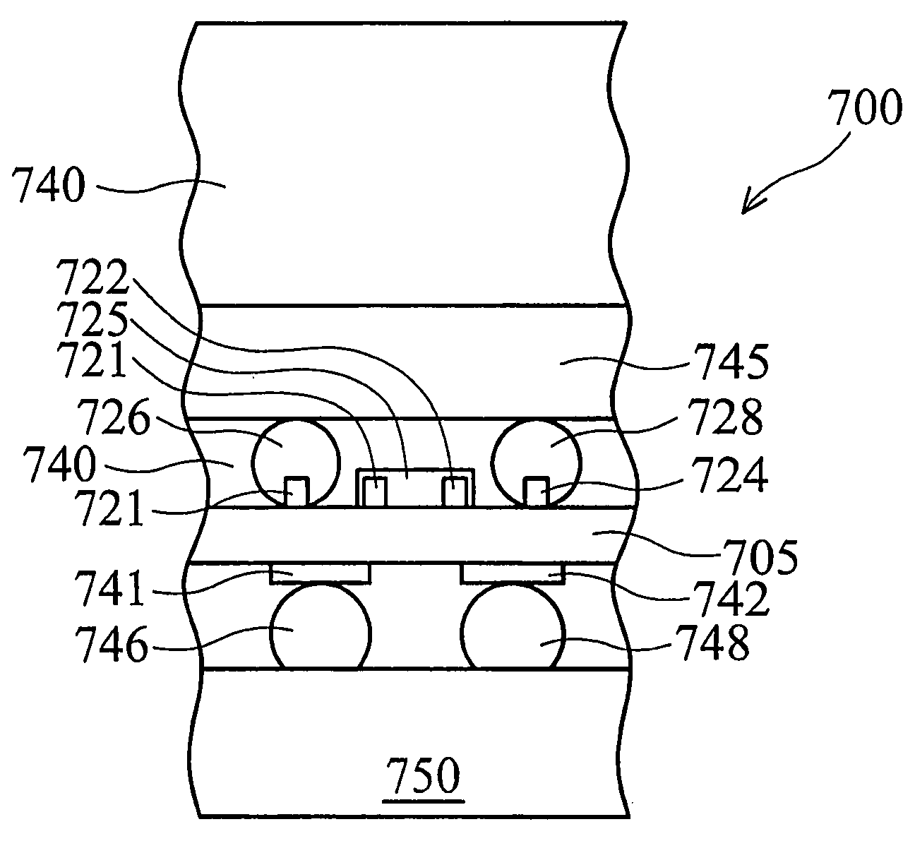
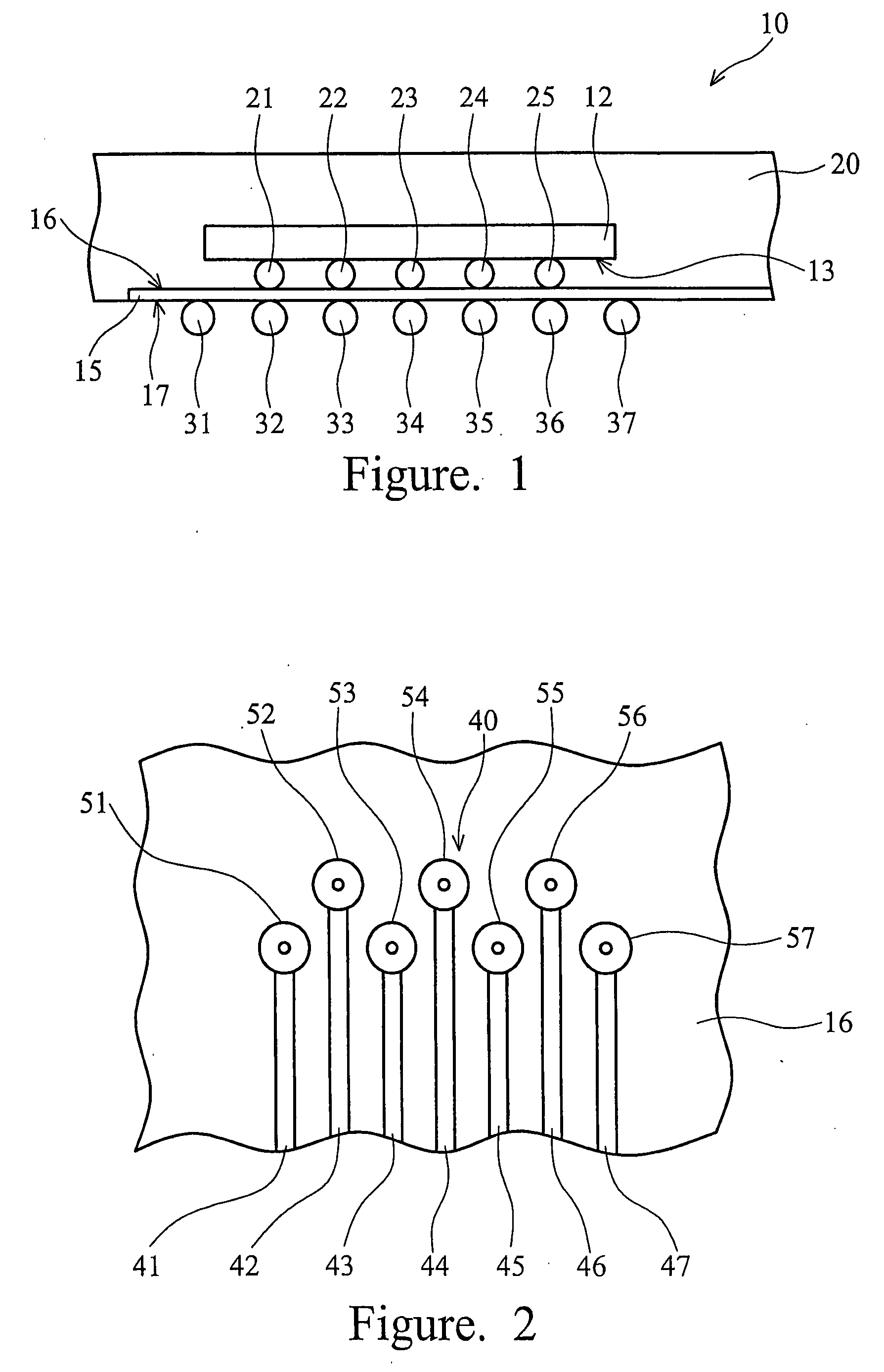
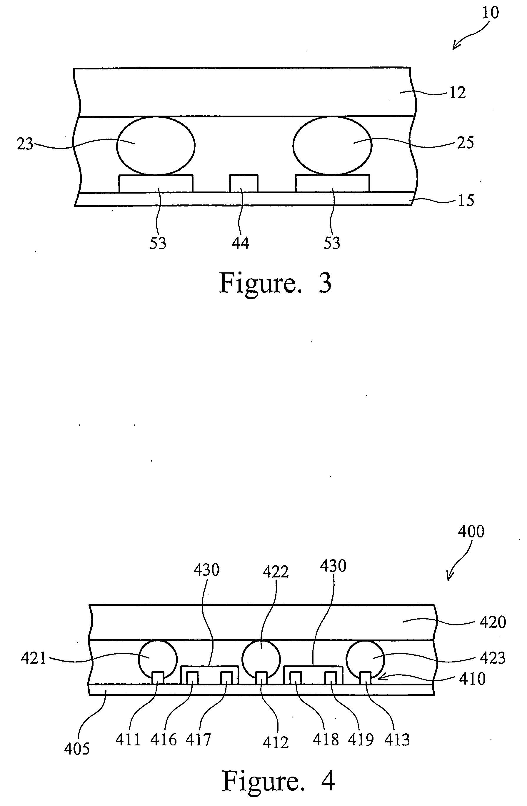
[0028]The present invention will be described with respect to preferred embodiments in a specific context, namely, where the active surface of a die is one upon which the electrical components of the device have been fabricated. (Although not typical or shown here, electrical components may be fabricated on other areas of the die as well, creating more than one active surface.) The invention may also be applied, however, to other semiconductor devices as well.

[0029]The present invention, then, is directed to a low cost substrate design especially advantageous for use in a fli...


PUM


Abstract

A novel design and method of fabricating a semiconductor device. In a preferred embodiment, the present invention is a flip chip package including a BT substrate. On the side of the substrate facing the die, thin traces are formed of an enhanced conductive material. Conductive bumps such as eutectic solder balls are then mounted on the traces, and the die mounted to the bumps. The die then packaged and mounted to a printed circuit board using, for example, a ball grid array.

Description

TECHNICAL FIELD[0001]The present invention relates generally to the field of semiconductor chip package design, and relates more particularly to a novel substrate design that is especially advantageous when implemented in a flip chip package.BACKGROUND[0002]A flip chip is a type of semiconductor device. Semiconductor devices are very small electrical components interconnected into integrated circuits that perform various computing and memory functions necessary to the generation of modern electronic appliances. Appliances based on semiconductor devices include personal computers, mobile telephones, and personal entertainment devices, as well as many others. Not only are such appliances popular, but advances in materials, design, and fabrication technology have made them more affordable for the average consumer. This affordability has in turn enabled many additional applications for use of semiconductor devices and, of course, increased their popularity even more.[0003]In general, se...

Claims


Application Information

Patent Timeline
IPC IPC(8): H01L23/488H01L21/441H01L21/60
CPCH01L23/49816H01L23/5386H01L24/11H01L24/12H01L24/16H01L2224/13099H01L2924/01002H01L2924/01015H01L2924/01029H01L2924/01033H01L2924/01075H01L2924/01078H01L2924/01082H01L2924/01322H01L2924/14H01L2924/19043H01L2924/01006H01L2924/014H01L2224/131H01L2924/00011H01L2924/00014H01L2924/00H01L2224/0401
Inventor SU, CHAO-YUANHSU, CHIA HSIUNGHSU, STEVEN
Owner TAIWAN SEMICON MFG CO LTD
Why Eureka
Try Eureka