Lamp heating apparatus and method for producing semiconductor device

a technology of heating apparatus and semiconductor device, which is applied in the direction of light heating apparatus, drying machine, drying, etc., can solve the problems of changing device performance, affecting the stability of temperature measurement and temperature control, and affecting the uniformity of temperature throughout the wafer plan

Inactive Publication Date: 2008-10-09
SHARP KK
View PDF4 Cites 9 Cited by
  • Summary
  • Abstract
  • Description
  • Claims
  • Application Information

AI Technical Summary

Benefits of technology

[0042]According to the present invention, since, in an RTA processing apparatus, between substrate processings, a radical of oxygen, hydrogen, a fluorocarbon compound, or the like is supplied from the outside of the chamber into the inside thereof, contaminated substances contaminated by dopants such as phosphorus, arsenic, and boron, which occur upon heat processing, are cleaned away in-situ. In addition, since no plasma occurs in the inside of the chamber, there is no physical damage resulting from plasma irradiation, and the transparent window and the surface of the sensing portion do not become rough. As a result, the measurement system associated with temperature control of the substrate is stabilized, and temperature uniformity and reproductivity of heat processing conditions are made better, leading to improved process stability. Further, there are such advantageous effects that the inside of the chamber is kept clean and the occurrence of foreign substances such as particles is inhibited.
that the inside of the chamber is kept clean and the occurrence of foreign substances such as particles is inhibited.

Problems solved by technology

In particular, if diffusing substances such as P, As, and B attach to and accumulate on the temperature sensor, and the sensing portion becomes cloudy, stability in temperature measuring and temperature control is undermined, thus making temperature uniformity throughout the wafer plane and temperature reproductivity for each processing impossible.
This causes a change in device performance, making it impossible to obtain products as designed.
Thus, there is an increasing risk of the above-described cloud.
However, this method eventually causes a reduction in time of operation of the apparatus.
In addition, the period of time of regular processing between cleaning processings is affected by cloud that occurs with time.
However, although the above-described method is effective for inhibiting the occurrence of sublimation substances on the rear surface of wafer 1, transparent window 15 at the front side of wafer is not taken into consideration.
In addition, it is not desirable to introduce an oxidizing gas that can be involved in processing for the purpose of cleaning when wafer 1 is in a state of being provided in chamber 30, in that in terms of control of process where miniaturization is being promoted, even if the oxidizing gas is in a minute amount, there is a possibility of being affected by turning-around of the oxidizing gas.

Method used


Image

  • Lamp heating apparatus and method for producing semiconductor device
  • Lamp heating apparatus and method for producing semiconductor device
  • Lamp heating apparatus and method for producing semiconductor device

Examples


Embodiment Construction

[0046]The object of providing a lamp heating apparatus that stabilizes the measurement system associated with temperature control of the substrate has been realized by such a structure that the inside of the chamber is cleaned with the use of a radical when the cloudy state of the transparent window and the surface of the sensing portion exceeds a predetermined cloudy state, and that a series of operations comprising heat annealing of the substrate and cleaning of the inside of the chamber is made possible. An embodiment of the present invention will be described below referring to the drawings.

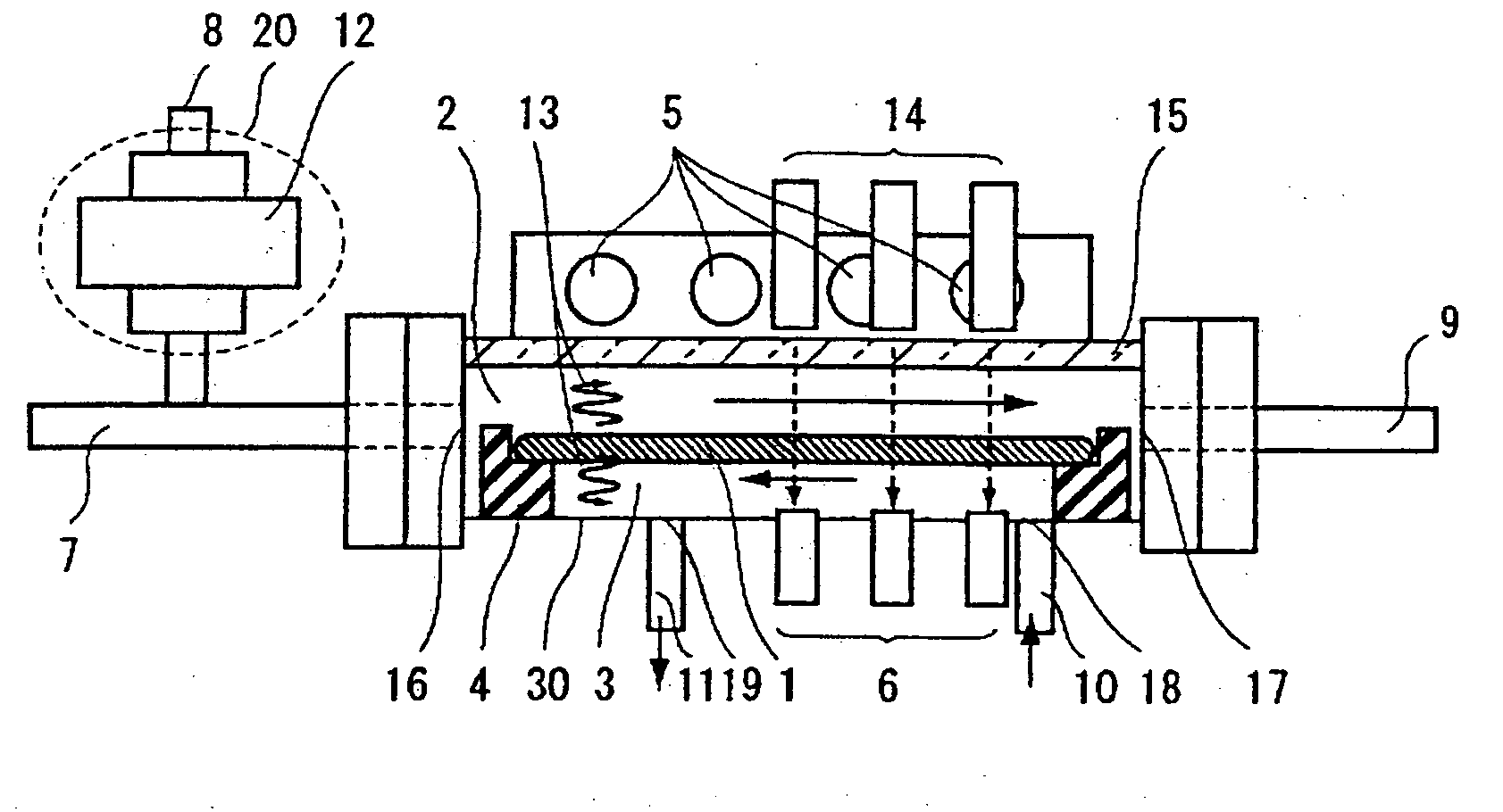
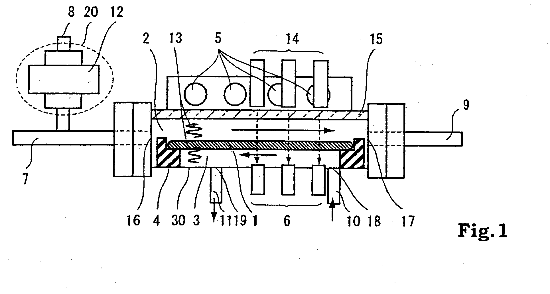
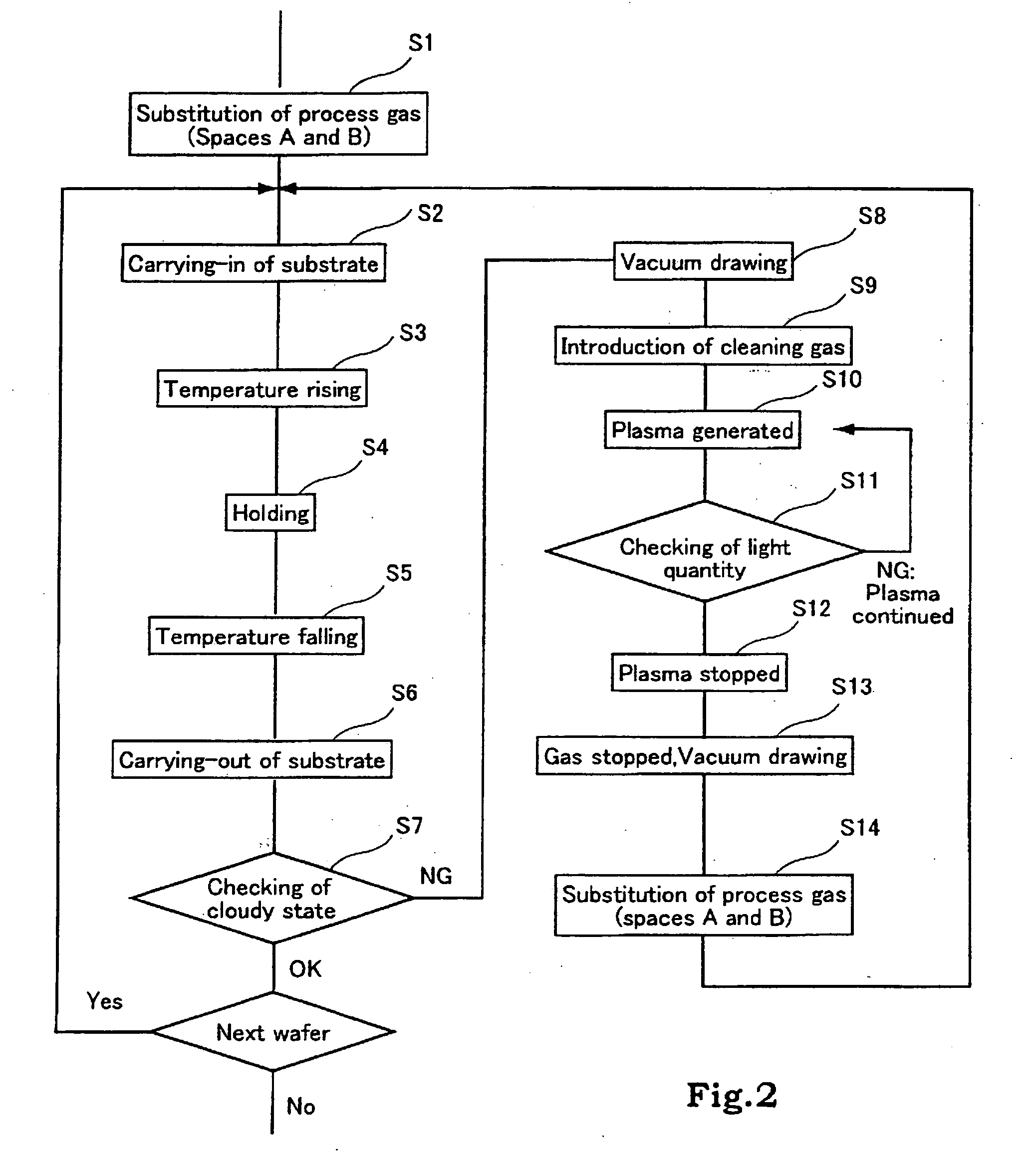
[0047]FIG. 1 is a schematic cross-section of a heat processing apparatus according to the present invention. FIG. 2 is a flow chart showing a method of producing a semiconductor device with the use of the lamp heating apparatus. In FIGS. 1 and 3, like parts in the figures are denoted by like reference numbers.

[0048]A lamp heating apparatus according to this embodiment has chamber 30 that has ...


PUM


Abstract

A lamp heating apparatus has: a chamber having a transparent window and housing a substrate; a heating lamp for heating the substrate by radiant heat of a heating lamp through the transparent window; a radiation thermometer that optically detects the temperature of the substrate and has a sensing portion provided in the chamber; a radical generating portion for generating a radical outside the chamber and supplying the radical into the chamber; and a light quantity sensor for determining the time for cleaning the inside of the chamber from a cloudy state of the transparent window and the surface of the sensing portion. This lamp heating apparatus enables a series of operations including heat annealing of the substrate and cleaning of the inside of the chamber. According to this invention, a lamp heating apparatus that has good temperature uniformity and reproductivity of heat processing conditions is obtained.

Description

[0001]This non-provisional application claims priority under 35 U.S.C. §119(a) on Japanese Patent Application No. 2004-273548 filed in Japan on Sep. 21, the entire contents of which are hereby incorporated by reference.BACKGROUND OF THE INVENTION[0002]1) Field of the Invention[0003]The present invention generally relates to lamp heating apparatuses, and more particularly to a lamp heating apparatuses for rapidly heating the substrate when producing a semiconductor device. The present invention also relates to a method for producing a semiconductor device by using the lamp heating apparatuses.[0004]2) Description of the Related Art[0005]For heat processing that is used in producing semiconductor devices represented by memories and logics, roughly speaking, furnaces and RTA (rapid thermal annealing) are used. In particular, in recent years, miniaturization and thinning of the devices is being promoted very rapidly, and accordingly creating a need for a reduction in the thermal history...

Claims


Application Information

Patent Timeline
Patent Type & Authority Applications(United States)
IPC IPC(8): F26B19/00
CPCH01L21/67115
Inventor SOHTOME, YOSHIHIRO
Owner SHARP KK
Why Eureka
Try Eureka