

Method for programming a semiconductor memory device
a memory device and semiconductor technology, applied in static storage, digital storage, instruments, etc., can solve the problems of affecting data reliability, interfering between adjacent cells affecting data threshold distribution, and taking a long time to program a certain data level
- Summary
- Abstract
- Description
- Claims
- Application Information
AI Technical Summary
Problems solved by technology
Method used
Image

Examples
embodiment 1
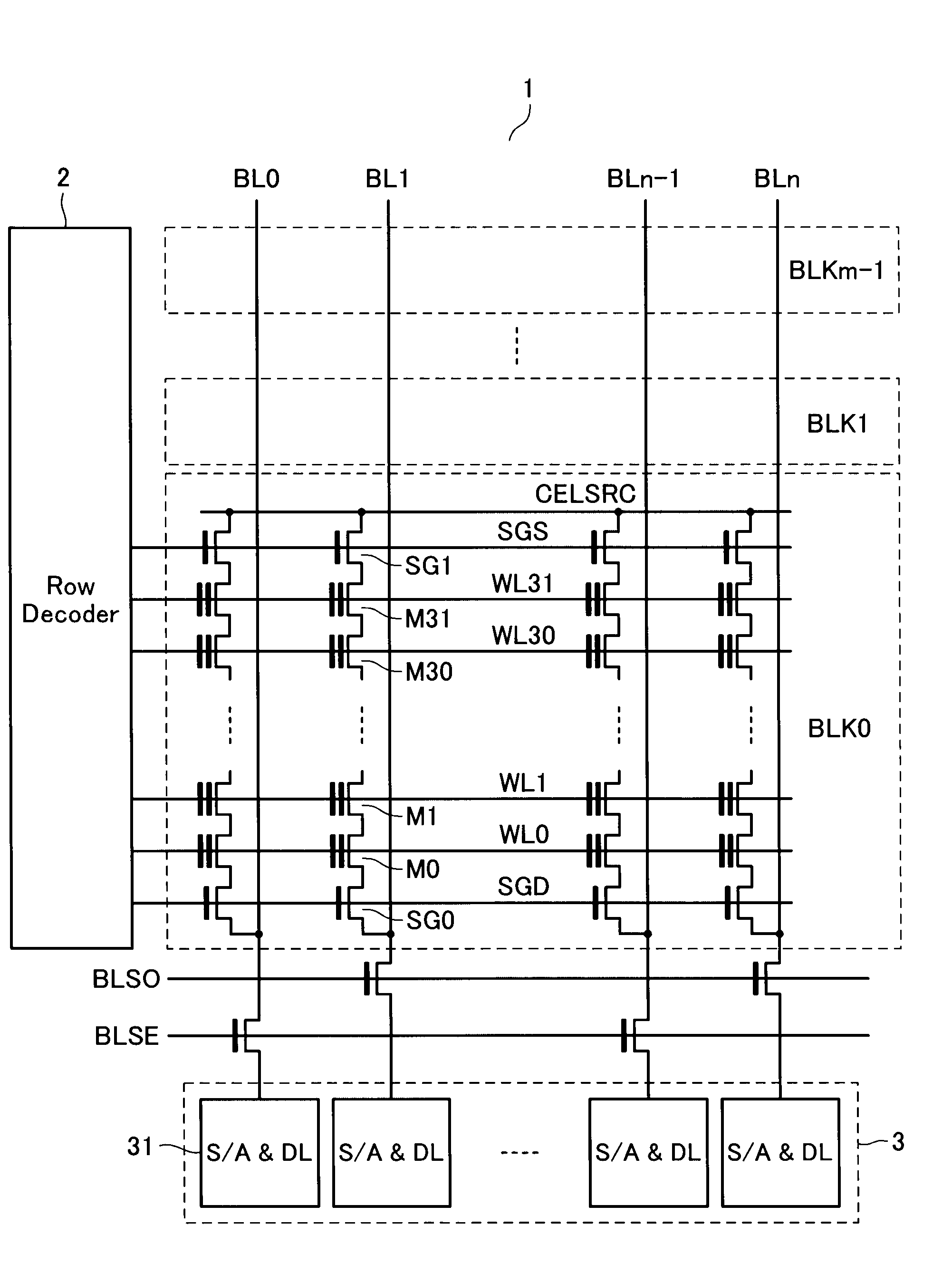
[0042]FIG. 1 shows a memory core in a NAND-type flash memory with a multi-level data storage scheme in accordance with an embodiment. Memory cell array 1 is formed of multiple NAND cell units (i.e., NAND strings), each having a plurality of electrically rewritable and non-volatile memory cells M0-M31.
[0043]One end of each NAND cell unit is coupled to a bit line BL via a select gate transistor SG0; and the other end to a cell source line CELSRC via another select gate transistor SG1. Control gates of the memory cells M0-M31 in the NAND cell unit are coupled to different word lines WL0-WL31, respectively. Gates of the select gate transistors SG0 and SG1 are coupled to select gate lines SGD and SGS, respectively, which run in parallel with the word lines.
[0044]To select and drive the word lines WL(WL0-WL31) and select gate lines SGD, SGS, there is disposed is a row decoder 2. Each bit line BL is coupled to a sense amplifier (serving as a data latch) 31 in a sense amplifier circuit 3.
[0...
embodiment 2
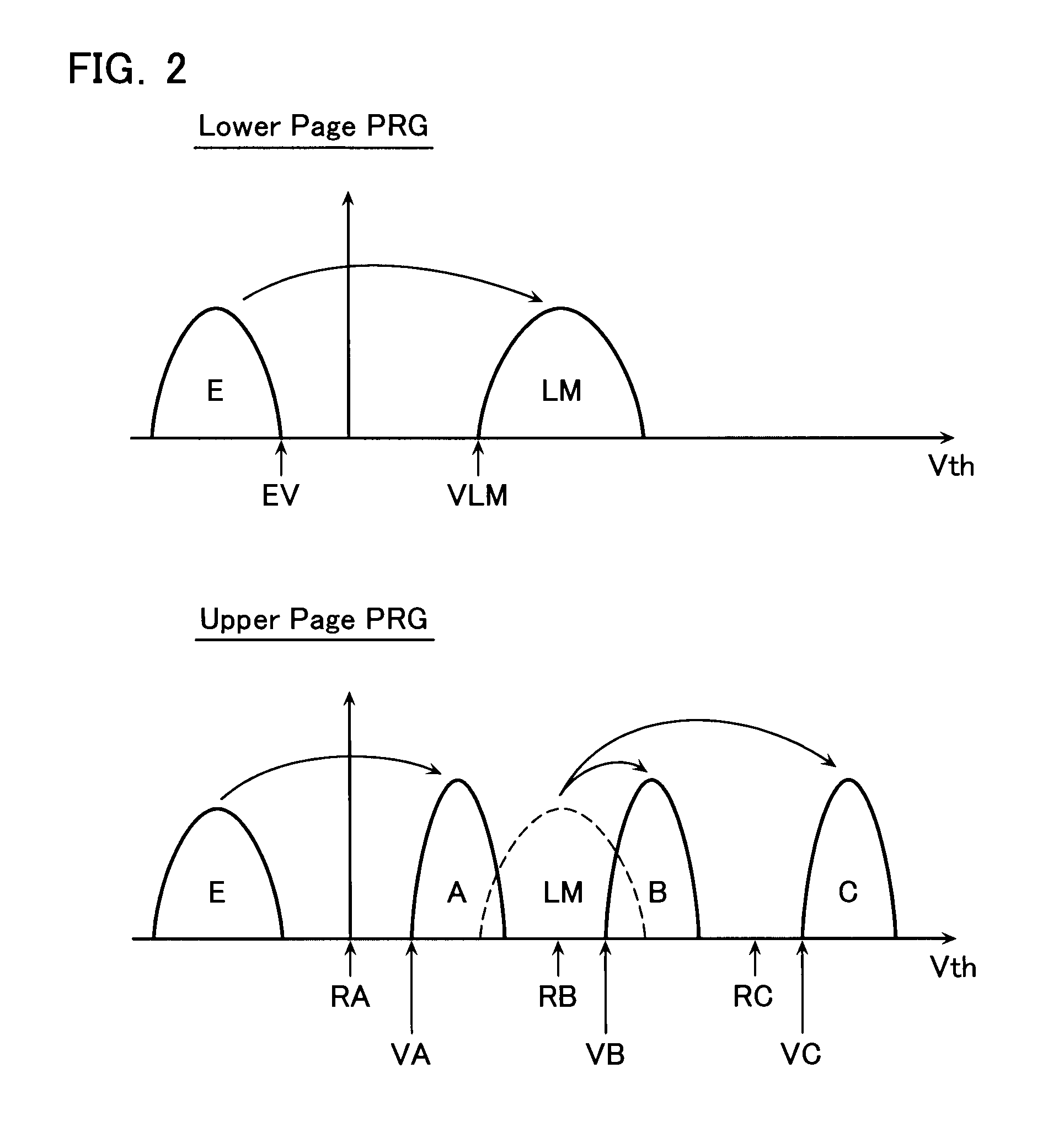
[0095]In the Embodiment 1, 4-level data program is performed with a lower page program for programming the medium level LM; and an upper page program. In this Embodiment 2, it will be explained such a program scheme that data states A, B and C are programmed directly from data state E, i.e., so-called “straight program scheme”.
[0096]FIG. 9 shows 4-level data E, A, B and C in the straight program scheme. This data level relationship itself is the same as that in the above-described Embodiment 1. Program (1) from data E to data C; program (2) from data E to data B; and program (3) from data E to data A, are sequentially performed in this embodiment.
[0097]FIG. 10 shows program voltage waveforms in this straight program scheme. Program (1) from data E to data C (i.e., C-PRG), program (2) from data E to data B (i.e., B-PRG) and program (3) from data E to data A (i.e., A-PRG) are performed similarly to the upper page program in the above-described embodiment.
[0098]Data program is performe...
embodiment 3
[0109]A program performance will be determined by that how many program cycles are required for programming a data threshold distribution. That is, the less the number of program cycles, the higher the program performance.
[0110]As shown in the expression (1), the number of the entire program cycles, CAVP, required for programming a threshold level is defined by the number of program cycles, CNVP, during there is no verify-passed cell, one pulse programming distribution width “vp1” and the program voltage step ΔVPGM. To make the waste program cycle number CNVP less, it is required to apply a suitable initial program voltage for obtaining a target threshold level. This will be solved in accordance with the methods explained in the Embodiments 1 and 2.
[0111]The step-up voltage ΔVPGM is determined by how wide is required for the final threshold distribution. In such a multi-level data storage NAND-type flash memory that stores n(≧2) bits / cell, it is required to arrange threshold distrib...
PUM
 Abstract
Description
Claims
Application Information